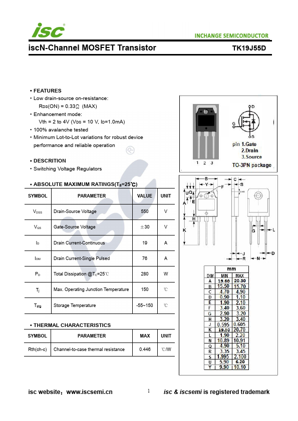
Click to expand full text
iscN-Channel MOSFET Transistor
TK19J55D
·FEATURES ·Low drain-source on-resistance:
RDS(ON) = 0.33Ω (MAX) ·Enhancement mode:
Vth = 2 to 4V (VDS = 10 V, ID=1.0mA) ·100% avalanche tested ·Minimum Lot-to-Lot variations for robust device
performance and reliable operation
·DESCRITION ·Switching Voltage Regulators
·ABSOLUTE MAXIMUM RATINGS(Ta=25℃)
SYMBOL
PARAMETER
VALUE
UNIT
VDSS
Drain-Source Voltage
550
V
VGS
Gate-Source Voltage
±30
V
ID
Drain Current-Continuous
19
A
IDM
Drain Current-Single Pulsed
76
A
PD
Total Dissipation @TC=25℃
280
W
Tj
Max. Operating Junction Temperature
150
℃
Tstg
Storage Temperature
-55~150 ℃
·THERMAL CHARACTERISTICS
SYMBOL
PARAMETER
Rth(ch-c) Channel-to-case thermal resistance
MAX 0.446
UNIT ℃/W
isc website:www.iscsemi.