DESCRIPTION
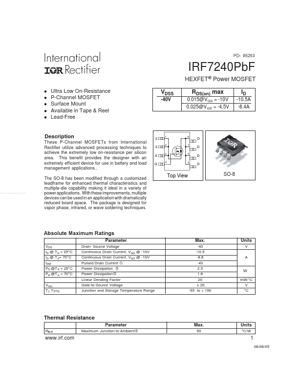
These P-Channel MOSFETs from International Rectifier utilize advanced processing techniques to achieve the extremely low on-resistance per silicon area. With these improvements, multiple devices can be used in an application with dramatically reduced board space. The package is designed for vapor phase, infrared, or wave soldering techniques. S 1 8 A D D D D S S G 2 7 3 6 4 5 Top View SO-8 ABSOLUTE MAXIMUM RATINGS
Parameter VDS ID @ TA = 25°C ID @ TA= 70°C IDM PD @TA = 25°C PD @TA = 70°C VGS TJ, TSTG Drain- Source Voltage Continuous Drain Current, VGS @ -10V Continuous Drain Current, VGS @ -10V Pulsed Drain Current Power Dissipation Power Dissipation Linear Derating Factor Gate-to-Source Voltage Junction and Storage Temperature Range Max. -40 -10.5 -8.6 -43 2.5 1.6 20 ± 20 -55 to + 150 Units V A W mW/°C V °C Thermal Resistance Parameter RθJA Maximum Junction-to-Ambient Max. 50 Units °C/W 1 06/06/05 IRF7240PbF ELECTRICAL CHARACTERISTICS
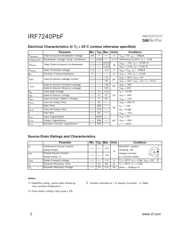
@ TJ = 25°C (unless otherwise specified) V(BR)DSS ∆V(BR)DSS/∆TJ Parameter Drain-to-Source Breakdown Voltage Breakdown Voltage Temp. International Rectifier