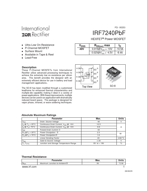
DESCRIPTION
S 1 These P-Channel MOSFETs from International Rectifier utilize advanced processing techniques to S 2 achieve the extremely low on-resistance per silicon area. A 8 D 7 D 6 D 5 D The SO-8 has been modified through a customized leadframe for enhanced thermal characteristics and multiple-die capability making it ideal in a variety of power applications. The package is designed for vapor phase, infrared, or wave soldering techniques. Top View SO-8 ABSOLUTE MAXIMUM RATINGS
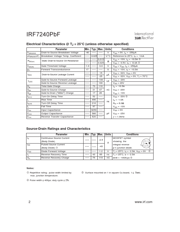
VDS ID @ TA = 25°C ID @ TA= 70°C IDM PD @TA = 25°C PD @TA = 70°C VGS TJ, TSTG Parameter Drain- Source Voltage Continuous Drain Current, VGS @ -10V Continuous Drain Current, VGS @ -10V Pulsed Drain Current Power Dissipation Power Dissipation Linear Derating Factor Gate-to-Source Voltage Junction and Storage Temperature Range Max. -40 -10.5 -8.6 -43 2.5 1.6 20 ± 20 -55 to + 150 Units V A W mW/°C V °C Thermal Resistance RθJA Parameter Maximum Junction-to-Ambient Max. 50 Units °C/W 1 06/06/05 IRF7240PbF Ele... International Rectifier