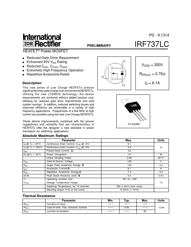
DESCRIPTION
Utilizing the new LCDMOS technology, the device improvements are achieved without added product cost, allowing for reduced gate drive requirements and total system savings. In addition, reduced switching losses and improved efficiency are achievable in a variety of high frequency applications. Frequencies of a few MHz at high current are possible using the new Low Charge MOSFETs. ABSOLUTE MAXIMUM RATINGS
Parameter ID @ TC = 25°C ID @ TC = 100°C IDM PD @TC = 25°C VGS EAS IAR EAR dv/dt TJ TSTG Continuous Drain Current, V GS @ 10V Continuous Drain Current, V GS @ 10V Pulsed Drain Current Power Dissipation Linear Derating Factor Gate-to-Source Voltage Single Pulse Avalanche Energy Avalanche Current Repetitive Avalanche Energy Peak Diode Recovery dv/dt Operating Junction and Storage Temperature Range Soldering Temperature, for 10 seconds Mounting torque, 6-32 or M3 screw. Max. 6.1 3.9 24 74 0.59 ±30 120 6.1 7.4 3.4 -55 to + 150 300 (1.6mm from case) 10 lbf●in (1.1N●m) Units A W... International Rectifier