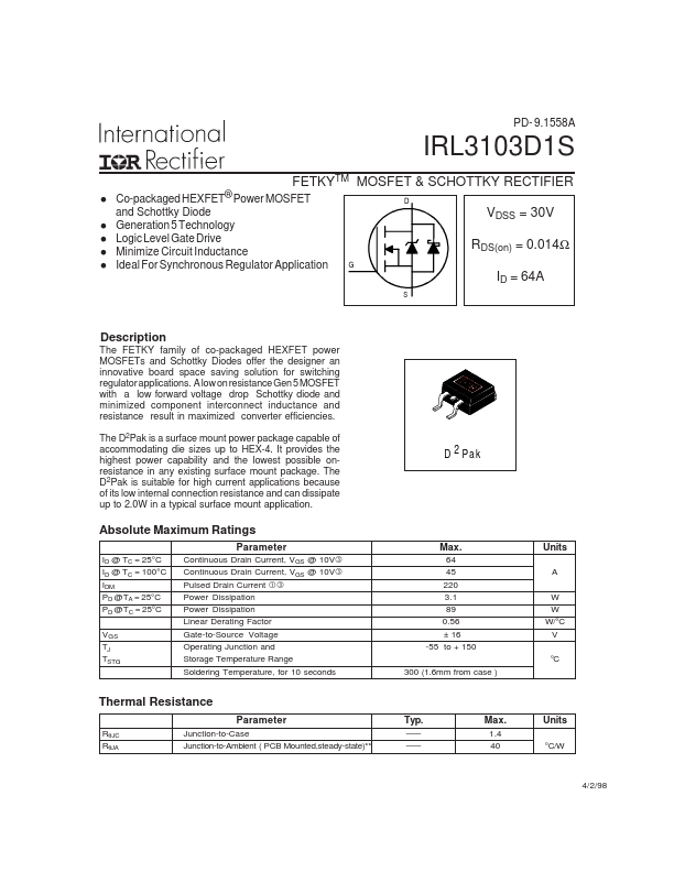
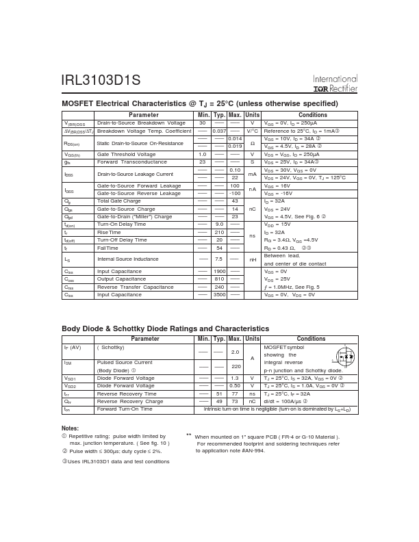
DESCRIPTION
A low on resistance Gen 5 MOSFET with a low forward voltage drop Schottky diode and minimized component interconnect inductance and resistance result in maximized converter efficiencies. It provides the highest power capability and the lowest possible onresistance in any existing surface mount package. The D2Pak is suitable for high current applications because of its low internal connection resistance and can dissipate up to 2.0W in a typical surface mount application. D 2 Pak T O -26 2 ABSOLUTE MAXIMUM RATINGS
Parameter ID @ TC = 25°C ID @ TC = 100°C IDM PD @TA = 25°C PD @TC = 25°C VGS TJ TSTG Continuous Drain Current, VGS @ 10V Continuous Drain Current, VGS @ 10V Pulsed Drain Current Power Dissipation Power Dissipation Linear Derating Factor Gate-to-Source Voltage Operating Junction and Storage Temperature Range Soldering Temperature, for 10 seconds Max. 64 45 220 3.1 89 0.56 ± 16 -55 to + 150 300 (1.6mm from case ) Units A W W W/°C V °C Thermal Resistance Parameter RθJC RθJA Junction-to-Case Junction-to-Ambient ( PCB Mounted,steady-state)** Typ. ––– ––– Max. International Rectifier