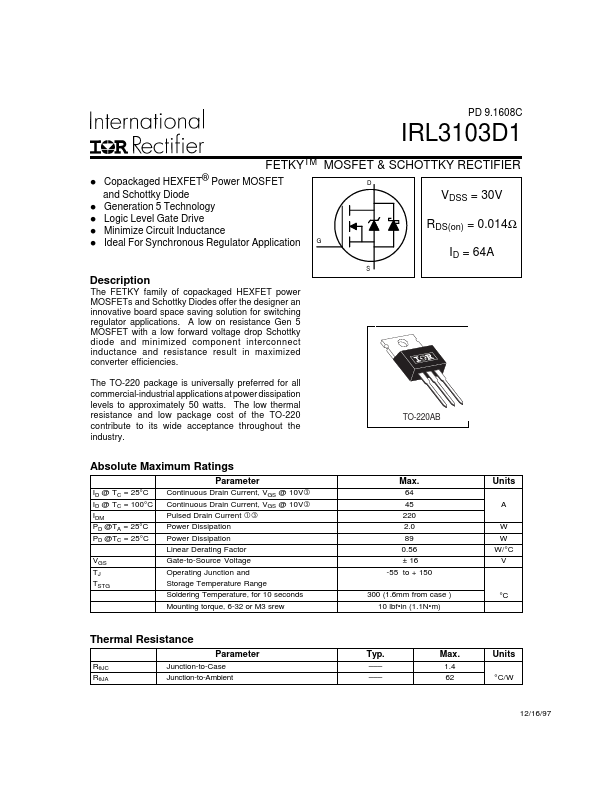
DESCRIPTION
A low on resistance Gen 5 MOSFET with a low forward voltage drop Schottky diode and minimized component interconnect inductance and resistance result in maximized converter efficiencies. The low thermal resistance and low package cost of the TO-220 contribute to its wide acceptance throughout the industry. TO-220AB ABSOLUTE MAXIMUM RATINGS
Parameter ID @ TC = 25°C ID @ TC = 100°C IDM PD @TA = 25°C PD @TC = 25°C VGS TJ TSTG Continuous Drain Current, VGS @ 10V Continuous Drain Current, VGS @ 10V Pulsed Drain Current Power Dissipation Power Dissipation Linear Derating Factor Gate-to-Source Voltage Operating Junction and Storage Temperature Range Soldering Temperature, for 10 seconds Mounting torque, 6-32 or M3 srew Max. 64 45 220 2.0 89 0.56 ± 16 -55 to + 150 300 (1.6mm from case ) 10 lbf●in (1.1N●m) Units A W W W/°C V °C Thermal Resistance Parameter RθJC RθJA Junction-to-Case Junction-to-Ambient Typ. ––– ––– Max. 1.4 62 Units °C/W 12/16/97 IRL3103D1 MOSFET ELECTRICAL CHARACTERISTICS
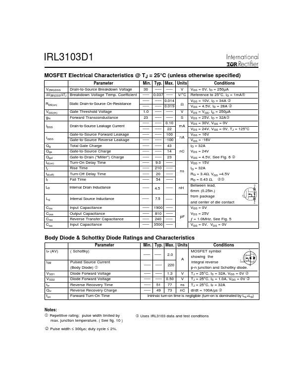
@ TJ = 25°C (unless otherwise specified) V(BR)DSS ∆V(BR)DSS/∆TJ Parameter Drain-to-Source Breakdown Voltage Breakdown Voltage Temp. International Rectifier