Datasheet Summary
IS43/46DR81280B(L), IS43/46DR16640B(L)
1Gb (x8, x16) DDR2 SDRAM
MARCH 2015
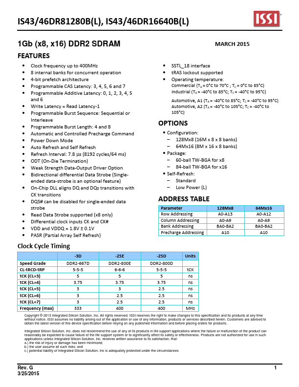
Features
- Clock frequency up to 400MHz
- 8 internal banks for concurrent operation
- 4-bit prefetch architecture
- Programmable CAS Latency: 3, 4, 5, 6 and 7
- Programmable Additive Latency: 0, 1, 2, 3, 4, 5 and 6
- Write Latency = Read Latency-1
- Programmable Burst Sequence: Sequential or
Interleave
- Programmable Burst Length: 4 and 8
- Automatic and Controlled Precharge mand
- Power Down Mode
- Auto Refresh and Self Refresh
- Refresh Interval: 7.8 s (8192 cycles/64 ms)
- ODT (On-Die Termination)
- Weak Strength Data-Output Driver Option
- Bidirectional differential Data Strobe (Single- ended data-strobe...