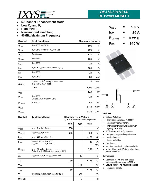
Datasheet4U Logo Datasheet4U.com

DE375-501N21A - RF Power MOSFET

Key Features

  • Test Conditions Characteristic Values TJ = 25°C unless otherwise specified min. VDSS VGS(th) IGSS IDSS RDS(on) gfs TJ TJM Tstg TL Weight 1.6mm (0.063 in) from case for 10 s VGS = 0 V, ID = 3 ma VDS = VGS, ID = 4 ma VGS = ±20 VDC, VDS = 0 VDS = 0.8 VDSS TJ = 25°C VGS = 0 TJ = 125°C VGS = 15 V, ID = 0.5ID25 Pulse test, t ≤ 300µS, duty cycle d ≤ 2% VDS = 15 V, ID = 0.5ID25, pulse test typ. max. V 5.5 ±100 50 1 0.22 V nA µA mA Ω S +175 °C °C +175 °C °C g 500 2.5.
  • Isolated Substrate.

📥 Download Datasheet

Full PDF Text Transcription (Reference)

The following content is an automatically extracted verbatim text from the original manufacturer datasheet and is provided for reference purposes only.

View original datasheet text
DE375-501N21A RF Power MOSFET ♦ ♦ ♦ ♦ ♦ N-Channel Enhancement Mode Low Qg and Rg High dv/dt Nanosecond Switching 50MHz Maximum Frequency Test Conditions TJ = 25°C to 150°C TJ = 25°C to 150°C; RGS = 1 MΩ Continuous Transient Tc = 25°C Tc = 25°C, pulse width limited by TJM Tc = 25°C Tc = 25°C IS ≤ IDM, di/dt ≤ 100A/µs, VDD ≤ VDSS, Tj ≤ 150°C, RG = 0.2Ω IS = 0 VDSS ID25 Maximum Ratings 500 500 ±20 ±30 25 150 21 30 5 >200 940 V V V V A A A mJ V/ns V/ns W W W C/W C/W SG1 SG2 GATE = = = = 500 V 25 A 0.22 Ω 940 W Symbol VDSS VDGR VGS VGSM ID25 IDM IAR EAR dv/dt PDC PDHS PDAMB RthJC RthJHS Symbol RDS(on) PDC DRAIN Tc = 25°C Derate 3.7W/°C above 25°C Tc = 25°C 425 4.5 0.16 0.36 SD1 SD2 Features Test Conditions Characteristic Values TJ = 25°C unless otherwise specified min.