DE150-501N04A Overview
Key Specifications
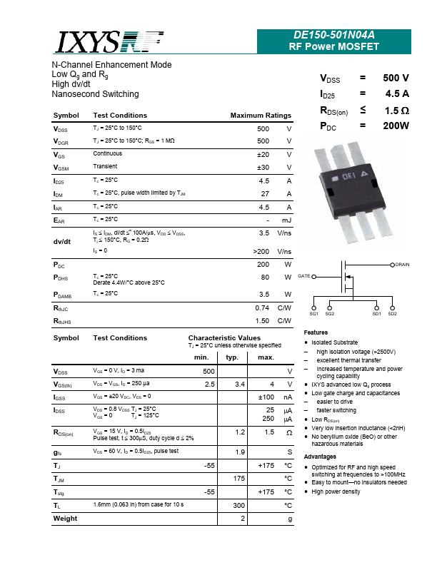
Pins: 6
Max Operating Temp: 175 °C
Min Operating Temp: -55 °C
Key Features
- Isolated Substrate
- high isolation voltage (>2500V)
- excellent thermal transfer
- Increased temperature and power cycling capability
- IXYS advanced low Qg process
- Low gate charge and capacitances
- easier to drive
- faster switching
- Very low insertion inductance (<2nH)
- No beryllium oxide (BeO) or other hazardous materials Advantages