Datasheet4U Logo Datasheet4U.com

IX4351NE - 9A Low Side SiC MOSFET/IGBT

General Description

The IX4351NE is designed specifically to drive SiC MOSFETs and high power IGBTs.

Separate 9A source and sink outputs allow for tailored turn-on and turn-off timing while minimizing switching losses.

Key Features

  • Separate 9A peak source and sink outputs.
  • Operating Voltage Range: -10V to +25V.
  • Internal charge pump regulator for selectable negative gate drive bias.
  • Desaturation detection with soft shutdown sink driver.
  • TTL and CMOS compatible input.
  • Under Voltage lockout (UVLO).
  • Thermal shutdown.
  • Open drain FAULT output.

📥 Download Datasheet

Full PDF Text Transcription (Reference)

The following content is an automatically extracted verbatim text from the original manufacturer datasheet and is provided for reference purposes only.

View original datasheet text
INTEGRATED CIRCUITS DIVISION Features • Separate 9A peak source and sink outputs • Operating Voltage Range: -10V to +25V • Internal charge pump regulator for selectable negative gate drive bias • Desaturation detection with soft shutdown sink driver • TTL and CMOS compatible input • Under Voltage lockout (UVLO) • Thermal shutdown • Open drain FAULT output Applications • Driving SiC MOSFETs and IGBTs • On-board charger and DC charging station • Industrial inverters • PFC, AC/DC and DC/DC converters 
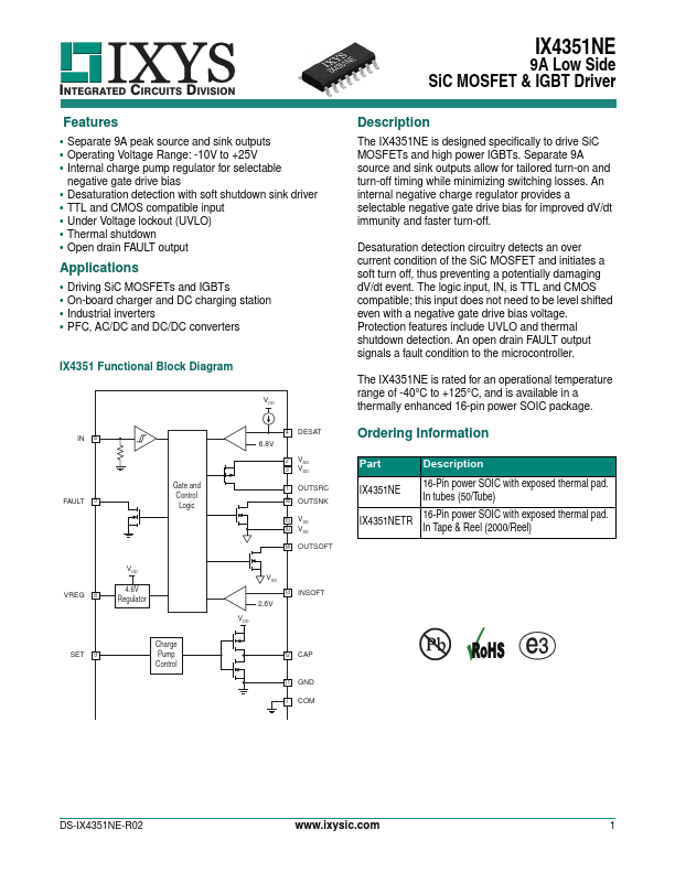
IX4351 Functional Block Diagram IN 6 FAULT 5 Gate and Control Logic VREG 8 VDD 4.6V Regulator SET 9 Charge Pump Control VDD 6.8V 4 DESAT 2 VDD 3 VDD 1 OUTSRC 16 OUTSNK 15 VSS 10 VSS 14 OUTSOFT V SS 13 INSOFT 2.