2SK1082 Overview
Key Specifications
Description
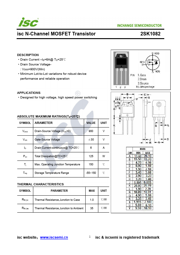
Drain Current –ID=6A@ TC=25℃ - Drain Source Voltage- : VDSS=900V(Min) - Minimum Lot-to-Lot variations for robust device performance and reliable operation.
| Part | 2SK1082 |
|---|---|
| Description | N-Channel MOSFET Transistor |
| Category | MOSFET |
| Manufacturer | Inchange Semiconductor |
| Size | 203.81 KB |
Drain Current –ID=6A@ TC=25℃ - Drain Source Voltage- : VDSS=900V(Min) - Minimum Lot-to-Lot variations for robust device performance and reliable operation.
| Seller | Inventory | Price Breaks | Buy |
|---|---|---|---|
| No distributor offers were returned for this part. | |||
| Part Number | Manufacturer | Description |
|---|---|---|
| K1082 | Fuji Electric | 2SK1082 |
| 2SK1082 | Fuji Electric | N-Channel Silicon Power MOS-FET |
| 2SK1082-01 | Fuji Electric | N-Channel Silicon Power MOS-FET |
| K1086-MR | Fuji Electric | 2SK1086-MR |
| 2SK1088 | Fuji Electric | N-channel MOS-FET |