BTS781GP
BTS781GP is TrilithIC manufactured by Infineon.
Overview
Features
BTS 781 GP
Quad D-MOS switch Free configurable as bridge or quad-switch Optimized for DC motor management applications Low RDS ON: 26 mΩ high-side switch, 14 mΩ low-side switch (typical values @ 25 °C) Maximum peak current: typ. 42 A @ 25 °C= Very low quiescent current: typ. 4 µA @ 25 °C= Small outline, thermal optimized Power Pak Load and GND-short-circuit-protection Operates up to 40 V Status flag for over temperature Open load detection in Off-mode Overtemperature shut down with hysteresis Internal clamp diodes Isolated sources for external current sensing Under-voltage detection with hysteresis Ordering Code Q67006-A9526
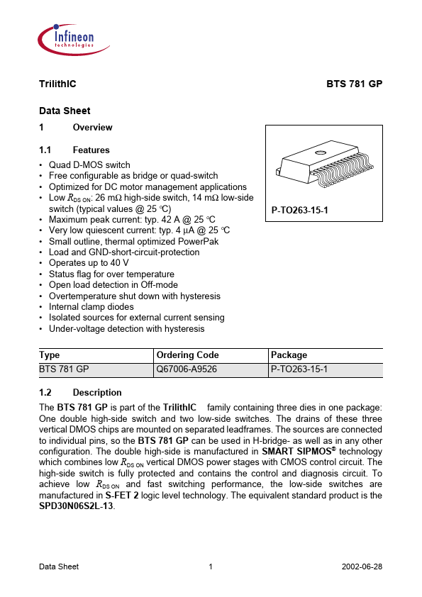
P-TO263-15-1
Type BTS 781 GP 1.2 Description
Package P-TO263-15-1
The BTS 781 GP is part of the Trilith IC family containing three dies in one package: One double high-side switch and two low-side switches. The drains of these three vertical DMOS chips are mounted on separated leadframes. The sources are connected to individual pins, so the BTS 781 GP can be used in H-bridge- as well as in any other configuration. The double high-side is manufactured in SMART SIPMOS® technology which bines low RDS ON vertical DMOS power stages with CMOS control circuit. The high-side switch is fully protected and contains the control and diagnosis circuit. To achieve low RDS ON and fast switching performance, the low-side switches are manufactured in S-FET 2 logic level technology. The equivalent standard product is the SPD30N06S2L-13.
Data Sheet
2002-06-28
BTS 781 GP
Pin Configuration (top view)
Molding pound NC SL1 IL1 NC IH1 ST1 SH1 DHVS GND IH2 ST2 SH2 SL2 NC IL2 1 Heat-Slug 1 2 18 3 4 5 Heat-Slug 2 6 7 8 9 10 11 12 Heat-Slug 3 13 16 14 15 DL2 17 DHVS DL1
Figure 1
Data Sheet
2002-06-28
BTS 781 GP
1.4 Pin No. 1 2 3 4 5 6 7 8 9 10 11 12 13 14 15 16 17 18
Pin Definitions and Functions Symbol NC SL1 IL1 NC IH1 ST1 SH1 DHVS GND IH2 ST2 SH2 SL2 NC IL2 DL2 DHVS DL1 Function Not connected Source of low-side switch 1...