SMBT3904PN
NPN/PNP Silicon Switching Transistor Array
High current gain Low collector-emitter saturation voltage Two (galvanic) internal isolated NPN/PNP
4 5 6
Transistors in one package
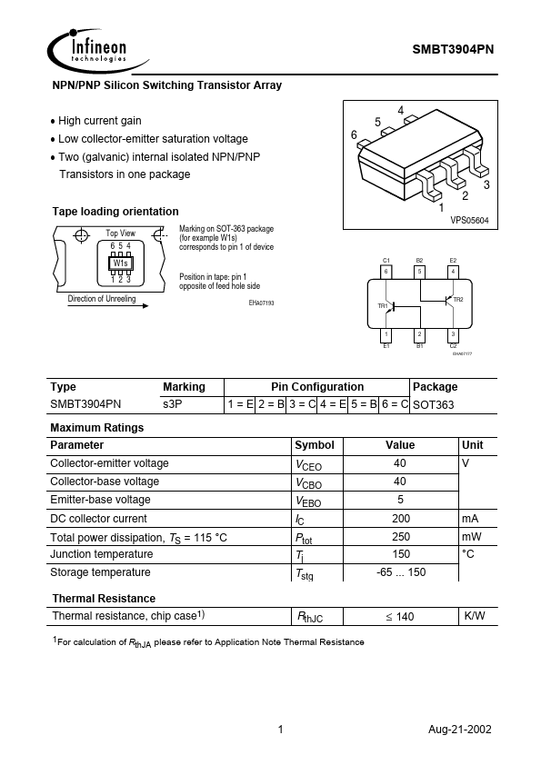
Tape loading orientation
Top View 6 5 4 W1s 1 2 3 Direction of Unreeling Position in tape: pin 1 opposite of feed hole side
EHA07193
VPS05604
Marking on SOT-363 package (for example W1s) corresponds to pin 1 of device
C1 6 B2 5 E2 4
TR2 TR1
1 E1
2 B1
3 C2
EHA07177
Type SMBT3904PN
Maximum Ratings Parameter
Marking s3P
Pin Configuration
Package
1 = E 2 = B 3 = C 4 = E 5 = B 6 = C SOT363
Symbol VCEO VCBO VEBO IC Ptot Tj Tstg Value 40 40 5 200 250 150 -65 ... 150 m A m W °C Unit V
Collector-emitter voltage Collector-base voltage Emitter-base voltage DC collector current Total power dissipation, TS = 115 °C Junction temperature Storage temperature Thermal Resistance
Thermal resistance, chip case1)
Rth JC
140
K/W
1For calculation of R th JA please refer to Application Note...