2EDF5215F
Features
- 250 V high and low-side gate driver
- -250 V negative HS transient immunity due to galvanic isolation
- 100 V/ns d V/dt robustness due to CT technology
- 5 A / 9 A source / sink capability
- +9 ns /-5 ns delay accuracy
- 4 ns maximum delay matching
- 1.2 V output clamping threshold in UVLO condition
- <2 μs fast start-up time in bootstrap operation
- Available in DSO-8 (5 mm x 6 mm) and VDSON-8 (4 mm x 4 mm)
Product validation Fully qualified for industrial grade applications.
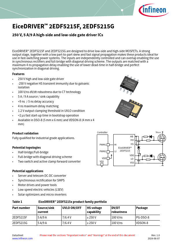
Controller
VBULK
HB HO
Potential topologies
- Half-bridge/Full-bridge
- Full-bridge with diagonal driving scheme
- Two switch and active clamp forward converter
PWM1
PWM2
VDD VSS
Eice DRIVER™
LI 2EDF5215
VDD LO
Potential applications
- Server and tele DC-DC converter
- Synchronous rectification for SMPS
- Motor drives and power tools
- Low-speed electric vehicles (LSEV)
- Solar optimizers and micro-inverters
Table 1 Part number
2EDF5215F 2EDF5215G
Eice DRIVER™ 2EDF5215x product...