Datasheet4U Logo Datasheet4U.com

BSO612CVG - Small-Signal-Transistor

Download the BSO612CVG datasheet PDF. This datasheet also covers the BSO612CV variant, as both devices belong to the same small-signal-transistor family and are provided as variant models within a single manufacturer datasheet.

Key Features

  • Dual N- and P -Channel.
  • Enhancement mode.
  • Avalanche rated Drain source voltage Drain-Source on-state resistance Continuous drain current.
  • Pb-free lead plating;RoHS compliant VDS RDS(on) ID N 60 0.12 3 P -60 V 0.3 W -2 A Type Package Marking BSO 612 CV PG-DSO-8 612CV Maximum Ratings,at Tj = 25 °C, unless otherwise specified Parameter Symbol Continuous drain current TA = 25 °C TA = 70 °C Pulsed drain current TA = 25 °C Avalanche energy, single pulse WID = 3 A, VD.

📥 Download Datasheet

Note: The manufacturer provides a single datasheet file (BSO612CV_InfineonTechnologiesAG.pdf) that lists specifications for multiple related part numbers.

Full PDF Text Transcription (Reference)

The following content is an automatically extracted verbatim text from the original manufacturer datasheet and is provided for reference purposes only.

View original datasheet text
Rev. 
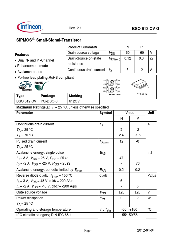
2.1 BSO 612 CV G SIPMOS® Small-Signal-Transistor Product Summary Features · Dual N- and P -Channel · Enhancement mode · Avalanche rated Drain source voltage Drain-Source on-state resistance Continuous drain current · Pb-free lead plating;RoHS compliant VDS RDS(on) ID N 60 0.12 3 P -60 V 0.