M2085
M2085 is VCSO FEC PLL WITH AUTOSWITCH FOR SONET/OTN manufactured by Integrated Circuit Solution Inc.
- Part of the M20 comparator family.
- Part of the M20 comparator family.
DESCRIPTION
The M2080/81/82 and M2085/86/87 are VCSO (Voltage Controlled SAW Oscillator) based clock PLLs designed for FEC clock ratio translation in 10Gb optical systems such as OC-192 or 10Gb E. They support FEC (Forward Error Correction) clock multiplication ratios, both forward (mapping) and inverse (de-mapping). Multiplication ratios are pin-selected from pre-programming look-up tables.
FEATURES
- Integrated SAW delay line; Output of 15 to 700 MHz
- - Low phase jitter < 0.5 ps rms typical (12k Hz to 20MHz or 50k Hz to 80MHz)
- LVPECL clock output (CML and LVDS options available)
- Pin-selectable PLL divider ratios support FEC ratios
- M2080/85: OTU1 (255/238) and OTU2 (255/237) Mapping
- M2081/86: OTU1 (238/255) or OTU2 (237/255) De-mapping
- M2082/87: OTU1 (238/255) and OTU2 (237/255) De-mapping
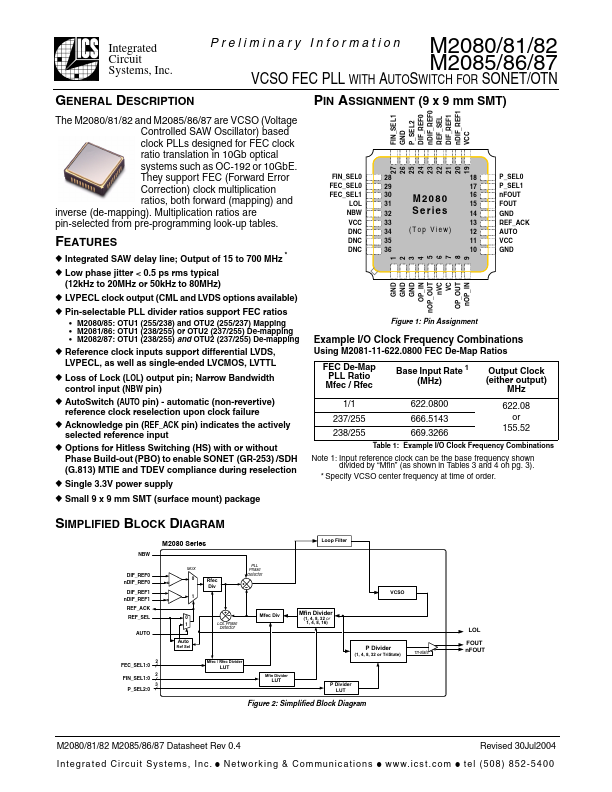
28 29 30 31 32 33 34 35 36
M2080 Series
(Top View)
18 17 16 15 14 13 12 11 10
P_SEL0 P_SEL1 n FOUT FOUT GND REF_ACK AUTO VCC GND
Figure 1: Pin Assignment
Example I/O Clock Frequency binations
Using M2081-11-622.0800 FEC De-Map Ratios FEC De-Map PLL Ratio Mfec / Rfec 1/1 237/255 238/255 Base Input Rate 1 (MHz) 622.0800 666.5143 669.3266 Output Clock (either output) MHz 622.08 or 155.52
- Reference clock inputs support differential LVDS, LVPECL, as well as single-ended LVCMOS, LVTTL
- Loss of Lock (LOL) output pin; Narrow Bandwidth control input (NBW pin)
- Auto Switch (AUTO pin)
- automatic (non-revertive) reference clock reselection upon clock failure
- Acknowledge pin (REF_ACK pin) indicates the actively selected reference input
- Options for Hitless Switching (HS) with or without Phase Build-out (PBO) to enable SONET (GR-253) /SDH (G.813) MTIE and TDEV pliance during reselection
- Single 3.3V power supply
- Small 9 x 9 mm SMT (surface mount) package
Table 1: Example I/O Clock Frequency binations
Note 1: Input reference clock can be the base frequency shown divided by “Mfin” (as shown in Tables 3 and 4 on pg. 3).
- Specify VCSO center frequency at time of...