ICS162834 Description
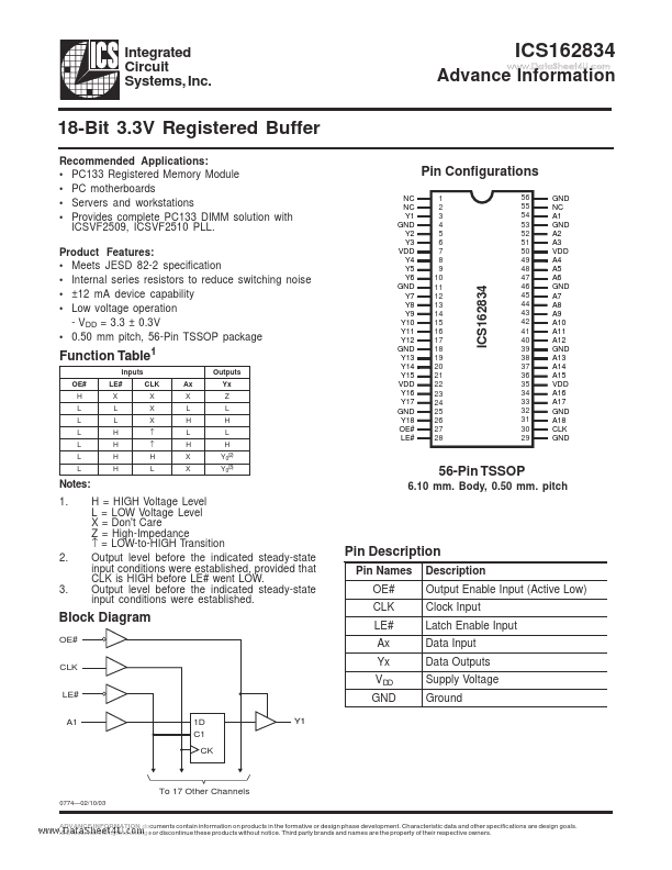
Pin Names OE# CLK LE# Ax Yx VDD GND Description Output Enable Input (Active Low) Clock Input Latch Enable Input Data Input Data Outputs Supply Voltage Ground Block Diagram OE# CLK LE# A1 1D C1 CK Y1 To 17 Other Channels 0774 02/10/03 ADVANCE INFORMATION documents contain information on products in the formative or design phase development. Characteristic data and other specifications are design goals. ICS reserves...
ICS162834 Key Features
- Meets JESD 82-2 specification
- Internal series resistors to reduce switching noise
- ±12 mA device capability
- Low voltage operation
- VDD = 3.3 ± 0.3V
- 0.50 mm pitch, 56-Pin TSSOP package 1