ICS8304I
ICS8304I is 1-TO-4 LVCMOS / LVTTL FANOUT BUFFER manufactured by Integrated Circuit Systems.
Integrated Circuit Systems, Inc.
LOW SKEW, 1-TO-4 LVCMOS / LVTTL FANOUT BUFFER
Features
- 4 LVCMOS / LVTTL outputs
- LVCMOS clock input
- CLK can accept the following input levels: LVCMOS, LVTTL
- Maximum output frequency: 166MHz
- Output skew: 60ps (maximum)
- Part-to-part skew: 650ps (maximum)
- Small 8 lead SOIC package saves board space
- 3.3V input, outputs may be either 3.3V or 2.5V supply modes
- -40°C to 85°C ambient operating temperature
GENERAL DESCRIPTION
The ICS8304I is a low skew, 1-to-4 Fanout Buffer and a member of the Hi Per Clock S™ Hi Per Clock S™ family of High Performance Clock Solutions from ICS. The ICS8304I is characterized at full 3.3V for input VDD, and mixed 3.3V and 2.5V for output operating supply modes (VDDO). Guaranteed output and part-to-part skew characteristics make the ICS8304I ideal for those clock distribution applications demanding well defined performance and .. repeatability.
,&6
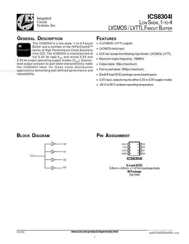
BLOCK DIAGRAM
Q0
PIN ASSIGNMENT
VDDO VDD CLK GND 1 2 3 4 8 7 6 5 Q3 Q2 Q1 Q0
Q1 CLK Q2
8-Lead SOIC 3.8mm x 4.8mm, x 1.47mm package body M Package Top View
Q3
8304AMI
.icst./products/hiperclocks.html
REV. B APRIL 4, 2002
Integrated Circuit Systems, Inc.
LOW SKEW, 1-TO-4 LVCMOS / LVTTL FANOUT BUFFER
Type Power Power Input Power Output Output Output Output Pulldown Description Output supply pin. Connect to 3.3V or 2.5V. Positive supply pin. Connect to 3.3V. LVCMOS / LVTTL clock input. Power supply ground. Connect to ground. Single clock output. LVCMOS / LVTTL interface levels. Single clock output. LVCMOS / LVTTL interface levels. Single clock output. LVCMOS / LVTTL interface levels. Single clock output. LVCMOS / LVTTL interface levels.
TABLE 1. PIN DESCRIPTIONS
Number 1 2 3 4...