ICS8304
ICS8304 is LOW SKEW / 1-TO-4 LVCMOS / LVTTL FANOUT BUFFER manufactured by Integrated Circuit Solution.
Integrated Circuit Systems, Inc.
LOW SKEW, 1-TO-4 LVCMOS / LVTTL FANOUT BUFFER
Features
- 4 LVCMOS / LVTTL outputs
- LVCMOS / LVTTL clock input
- Maximum output frequency: 200MHz
- Output skew: 45ps (maximum at 3.3V supply)
- Part-to-part skew: 500ps (maximum)
- Small 8 lead SOIC package saves board space
- 3.3V input, outputs may be either 3.3V or 2.5V supply modes
- Lead-Free package available
- 0°C to 70°C ambient operating temperature
GENERAL DESCRIPTION
The ICS8304 is a low skew, 1-to-4 Fanout Buffer and a member of the Hi Per Clock S ™ Hi Per Clock S™ family of High Performance Clock Solutions from ICS. The ICS8304 is characterized at full 3.3V for input VDD, and mixed 3.3V and 2.5V for output operating supply modes (VDDO). Guaranteed output and par t-to-par t skew character istics make the ICS8304 ideal for those clock distribution applications demanding well defined performance and repeatability.
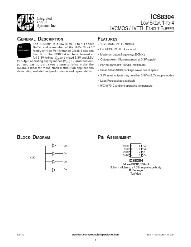
BLOCK DIAGRAM
Q0
PIN ASSIGNMENT
VDDO VDD CLK GND 1 2 3 4 8 7 6 5 Q3 Q2 Q1 Q0
Q1 CLK Q2
8-Lead SOIC, 150mil 3.9mm x 4.9mm, x 1.63mm package body M Package Top View
Q3
8304AM
.icst./products/hiperclocks.html
REV. F SEPTEMBER 13, 2004
Integrated Circuit Systems, Inc.
LOW SKEW, 1-TO-4 LVCMOS / LVTTL FANOUT BUFFER
Type Power Power Input Power Output Output Output Output Pulldown Description Output supply pin. Core supply pin. LVCMOS / LVTTL clock input. Power supply ground. Single clock output. LVCMOS / LVTTL interface levels. Single clock output. LVCMOS / LVTTL interface levels. Single clock output. LVCMOS / LVTTL interface levels. Single clock output. LVCMOS / LVTTL interface levels.
TABLE 1. PIN DESCRIPTIONS
Number 1 2 3 4 5 6 7 8 Name VDDO VDD CLK GND Q0 Q1 Q2 Q3
NOTE: Pulldown refers to internal input resistors. See Table 2, Pin Characteristics, for typical...