ICS83905I
ICS83905I is 1:6 CRYSTAL INTERFACE-TO LVCMOS/LVTTL FANOUT BUFFER manufactured by Integrated Circuit Systems.
Integrated Circuit Systems, Inc.
LOW SKEW, 1:6 CRYSTAL INTERFACE-TOLVCMOS / LVTTL FANOUT BUFFER
Features
- 6 LVCMOS / LVTTL outputs
- Outputs able to drive 12 series terminated lines
- Crystal oscillator interface
- Crystal input frequency range: 10MHz to 40MHz
- Output skew: 80ps (maximum)
- RMS phase jitter @ 25MHz, (100Hz
- 1MHz): 0.26ps (typical) (VDD = VDDO = 2.5V) Phase noise: Offset Noise Power 100Hz .............. -129.7 d Bc/Hz 1k Hz .............. -144.4 d Bc/Hz 10k Hz .............. -147.3 d Bc/Hz 100k Hz .............. -157.3 d Bc/Hz
- 5V tolerant enable inputs
- Synchronous output enables
- Operating power supply modes: Full 3.3V, 2.5V and 1.8V, mixed 3.3V core/2.5V output operating supply, mixed 3.3V core/1.8V output operating supply, mixed 2.5V core/1.8V output operating supply
- -40°C to 85°C ambient operating temperature
- Lead-Free package fully Ro HS pliant
GENERAL DESCRIPTION
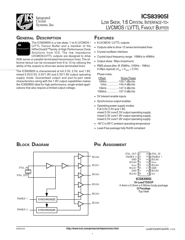
The ICS83905I is a low skew, 1-to-6 LVCMOS / LVTTL Fanout Buffer and a member of the Hi Per Clock S™ Hi Per Clock S™ family of High Performance Clock Solutions from ICS. The low impedance LVCMOS/LVTTL outputs are designed to drive 50W series or parallel terminated transmission lines. The effective fanout can be increased from 6 to 12 by utilizing the ability of the outputs to drive two series terminated lines.
..
The ICS83905I is characterized at full 3.3V, 2.5V, and 1.8V, mixed 3.3V/2.5V, 3.3V/1.8V and 2.5V/1.8V output operating supply mode. Guaranteed output and part-to-part skew characteristics along with the 1.8V output capabilities makes the ICS83905I ideal for high performance, single ended applications that also require a limited output voltage.
BLOCK DIAGRAM
PIN ASSIGNMENT
BCLK0 XTAL_OUT ENABLE 2 GND BCLK0 VDD o BCLK1 GND BCLK2 1 2 3 4 5 6 7 8 16 15 14 13 12 11 10 9 XTAL_IN ENABLE 1 BCLK5 VDDO BCLK4 GND BCLK3 VDD
BCLK1 XTAL_IN BCLK2
XTAL_OUT
BCLK3
16-Lead TSSOP 4.4mm x 5.0mm x 0.92mm body package G Pacakge Top View
BCLK4...