ICS9112-27
ICS9112-27 is Low Skew PCI/PCI-X Buffer manufactured by Integrated Circuit Systems.
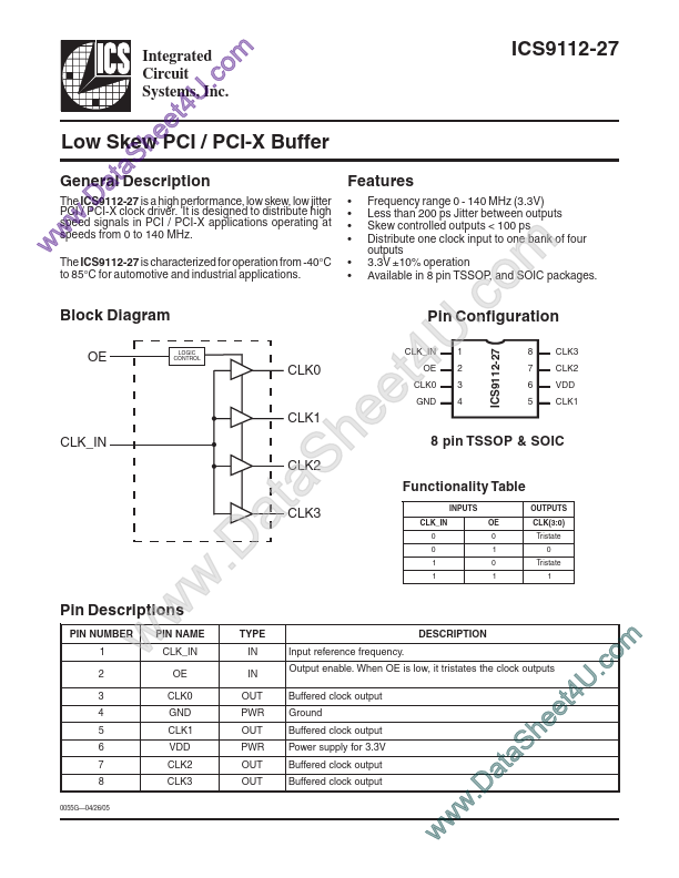
Integrated Circuit Systems, Inc. e e Low Skew PCI / PCI-X Buffer h S a tDescription General a The ICS9112-27 a high performance, low skew, low jitter .D clockisdriver. PCI / PCI-X It is designed to distribute high w speed signals in PCI / PCI-X applications operating at speeds w from 0 to 140 MHz. wThe ICS9112-27 is characterized for operation from -40°C to 85°C for automotive and industrial applications.
U 4 t
.c om
Features
- -
- -
- - Frequency range 0
- 140 MHz (3.3V) Less than 200 ps Jitter between outputs Skew controlled outputs < 100 ps Distribute one clock input to one bank of four outputs 3.3V ±10% operation Available in 8 pin TSSOP, and SOIC packages.
Block...