ICS91305I
ICS91305I is High Performance Communication Buffer manufactured by Integrated Circuit Systems.
Integrated Circuit Systems, Inc.
High Performance munication Buffer
General Description
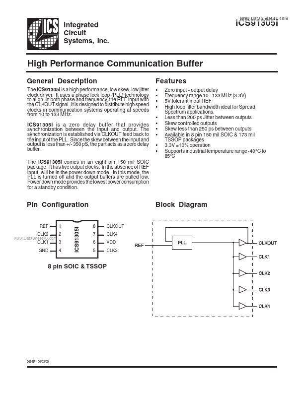
The ICS91305I is a high performance, low skew, low jitter clock driver. It uses a phase lock loop (PLL) technology to align, in both phase and frequency, the REF input with the CLKOUT signal. It is designed to distribute high speed clocks in munication systems operating at speeds from 10 to 133 MHz. ICS91305I is a zero delay buffer that provides synchronization between the input and output. The synchronization is established via CLKOUT feed back to the input of the PLL. Since the skew between the input and output is less than +/- 350 p S, the part acts as a zero delay buffer. The ICS91305I es in an eight pin 150 mil SOIC package. It has five output clocks. In the absence of REF input, will be in the power down mode. In this mode, the PLL is turned off and the output buffers are pulled low. Power down mode provides the lowest power consumption for a standby condition.
Features
- -
- -
- -
- -
- - Zero input
- output delay Frequency range 10
- 133 MHz (3.3V) 5V tolerant input REF High loop filter bandwidth ideal for Spread Spectrum applications. Less than 200 ps Jitter between outputs Skew controlled outputs Skew less than 250 ps between outputs Available in 8 pin 150 mil SOIC & 173 mil TSSOP packages 3.3V ±10% operation Supports industrial temperature range -40°C to 85°C
Pin Configuration
REF CLK2
..
Block Diagram
8 7 6 5 CLKOUT CLK4 VDD CLK3
2 3 4
CLK1 GND
8 pin SOIC & TSSOP
0691F- 06/03/05
Pin Descriptions
PIN NUMBER 1 2 3 4 5 6 7 8 PIN NAME REF
2 3 3
TYPE IN OUT OUT PWR OUT PWR
DESCRIPTION Input reference frequency, 5V tolerant input. Buffered clock output Buffered clock output Ground Buffered clock output Power Supply (3.3V) Buffered clock output Buffered clock output. Internal feedback on this pin
CLK2 CLK1
GND CLK3 VDD CLK4
3 3
OUT...