ICSLV810 Overview
Description
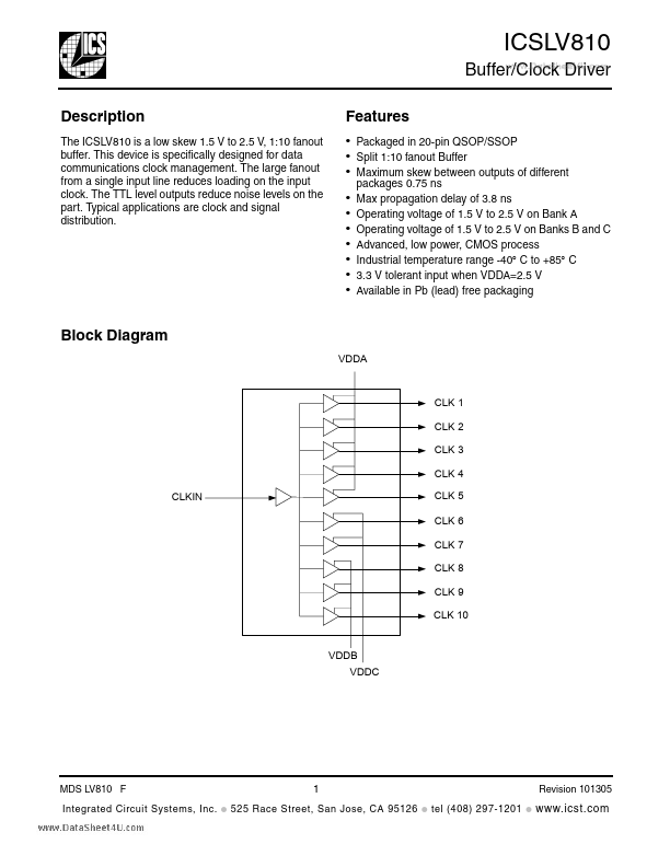
The ICSLV810 is a low skew 1.5 V to 2.5 V, 1:10 fanout buffer. This device is specifically designed for data communications clock management.
Key Features
- Packaged in 20-pin QSOP/SSOP
- Split 1:10 fanout Buffer
- Maximum skew between outputs of different