IDT72V8980
IDT72V8980 is 3.3 VOLT TIME SLOT INTERCHANGE DIGITAL SWITCH manufactured by Integrated Device Tech.
3.3 VOLT TIME SLOT INTERCHANGE DIGITAL SWITCH 256 x 256
Features
:
- -
- -
- -
- -
- -
256 x 256 channel non-blocking switch Serial Tele Bus patible (ST-BUS®) 8 RX inputs- 32 channels at 64 Kbit/s per serial line 8 TX output- 32 channels at 64 Kbit/s per serial line Three-state serial outputs Microprocessor Interface (8-bit data bus) 3.3V Power Supply Available in 44-pin Plastic Leaded Chip Carrier (PLCC), 48-pin Small Shrink Outline Package (SSOP), and 44-pin Plastic Quad Flatpack (PQFP) Operating Temperature Range -40° C to +85°C 3.3V I/O with 5V Tolerant Inputs and output channels. Those 256 channels are divided into 8 serial inputs and outputs, each of which consists of 32 channels (64 Kbit/s per channel) to form a multiplexed 2.048 Mb/s stream.
FUNCTIONAL DESCRIPTION
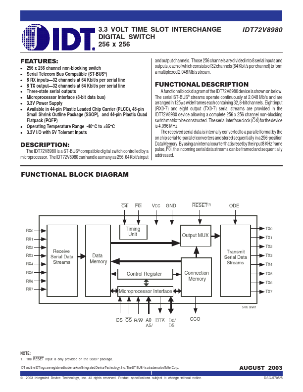
A functional block diagram of the IDT72V8980 device is shown on below. The serial ST-BUS® streams operate continuously at 2.048 Mb/s and are arranged in 125µs wide frames each containing 32, 8-bit channels. Eight input (RX0-7) and eight output (TX0-7) serial streams are provided in the IDT72V8980 device allowing a plete 256 x 256 channel non-blocking switch matrix to be constructed. The serial interface clock (C4i) for the device is 4.096 MHz. The received serial data is internally converted to a parallel format by the on chip serial-to-parallel converters and stored sequentially in a 256-position Data Memory. By using an internal counter that is reset by the input 8 KHz frame pulse, F0i, the ining serial data streams can be framed and sequentially addressed.
DESCRIPTION:
The IDT72V8980 is a ST-BUS® patible digital switch controlled by a microprocessor. The IDT72V8980 can handle as many as 256, 64 Kbit/s input
FUNCTIONAL BLOCK DIAGRAM
C4i
F0i
RESET(1)
RX0 RX1 RX2 RX3 RX4 RX5 RX6 RX7
Timing Unit
TX0
Output MUX
Transmit Serial Data Streams
TX1 TX2
Receive Serial Data Streams
Data Memory Control Register Connection Memory
TX3 TX4 TX5 TX6...