IDT72V8980
IDT72V8980 is 3.3 VOLT TIME SLOT INTERCHANGE DIGITAL SWITCH manufactured by Renesas.
3.3 VOLT TIME SLOT INTERCHANGE DIGITAL SWITCH 256 x 256
Features
:
- 256 x 256 channel non-blocking switch
- Serial Tele Bus patible (ST-BUS®)
- 8 RX inputs- 32 channels at 64 Kbit/s per serial line
- 8 TX output- 32 channels at 64 Kbit/s per serial line
- Three-state serial outputs
- Microprocessor Interface (8-bit data bus)
- 3.3V Power Supply
- Available in 44-pin Plastic Leaded Chip Carrier (PLCC), 48-pin
Small Shrink Outline Package (SSOP), and 44-pin Plastic Quad Flatpack (PQFP)
- Operating Temperature Range -40°C to +85°C
- 3.3V I/O with 5V Tolerant Inputs
DESCRIPTION:
The IDT72V8980 is a ST-BUS® patible digital switch controlled by a microprocessor. The IDT72V8980 can handle as many as 256, 64 Kbit/s input and output channels. Those 256 channels are divided into 8 serial inputs and outputs, each of which consists of 32 channels (64 Kbit/s per channel) to form a multiplexed 2.048 Mb/s stream.
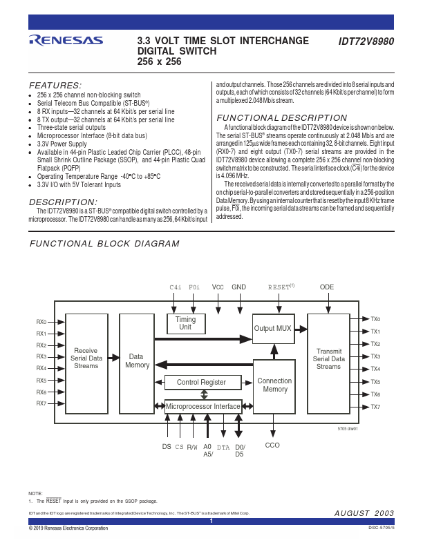
FUNCTIONAL DESCRIPTION
A functional block diagram of the IDT72V8980 device is shown on below. The serial ST-BUS® streams operate continuously at 2.048 Mb/s and are arranged in 125μs wide frames each containing 32, 8-bit channels. Eight input (RX0-7) and eight output (TX0-7) serial streams are provided in the IDT72V8980 device allowing a plete 256 x 256 channel non-blocking switch matrix to be constructed. The serial interface clock (C4i) for the device is 4.096 MHz.
The received serial data is internally converted to a parallel format by the on chip serial-to-parallel converters and stored sequentially in a 256-position Data Memory. By using an internal counter that is reset by the input 8 KHz frame pulse, F0i, the ining serial data streams can be framed and sequentially addressed.
FUNCTIONAL BLOCK DIAGRAM
C 4i F0i VCC GND
R ESET(1)
RX0
Timing
TX0
RX1
Unit
Output...