Integrated Device Technology 8T49N488
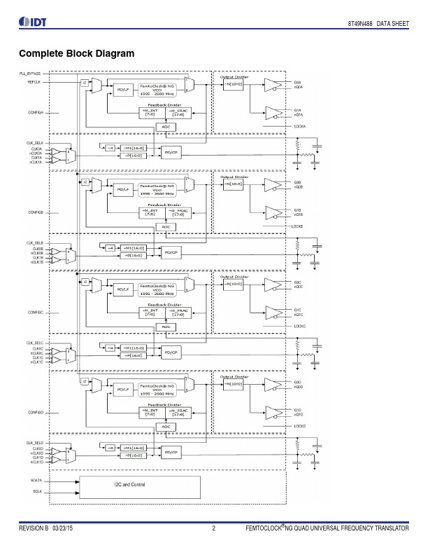
The 8T49N488 is a quad PLL with FemtoClock® NG technology, it integrates low phase noise Frequency Translator / Synthesizer, Jitter attenuation, and with alarm and monitoring functions suitable for networking and communications applications. Each PLL of 8T49N488 has three operating modes to support a very broad spectrum of applications: 1) Frequency Synthesizer • Synthesizes output frequencies from an external reference clock REFCLK.| Part No. | 8T49N488 |
|---|---|
| Datasheet | 8T49N488 Download |
| Manufacturer |  Integrated Device Technology |
| Description | NG QUAD Universal Frequency Translator |
| Buy | Stock & Price |
GENERAL DESCRIPTION
The device has four fully independent PLLs, each PLL is able to generate any output frequency in the 0.98MHz - 312.5MHz range and most output frequencies in the 312.5MHz - 1,300MHz range (see Table 3 for details). A wide range of input reference clocks and operation reference clock may be used as the source for the output frequency.● Fractional feedback division is used, so there are no requirements for any specific input reference clock frequency to produce the desired output frequency with a high degree of accuracy. 2) High-Bandwidth Frequency Translator
●
APPLICATIONS
: PCI Express, Computing, General Purpose● Translates any input clock in the 16MHz - 710MHz frequency range into any supported output frequency.
● This mode has a high PLL loop bandwidth in order to track input reference changes, such as Spread-Spectrum Clock modulation. 3) Low-Bandwidth Frequency Translator
●
APPLICATIONS
: Networking & Communications.● Translates any input clock in the 8kHz -710MHz frequency range into any supported output frequency.