ICS83948I
ICS83948I is 1-TO-12 DIFFERENTIALTO-LVCMOS/LVTTL FANOUT BUFFER manufactured by Integrated Device Technology.
LOW SKEW, 1-TO-12 DIFFERENTIALTO-LVCMOS/LVTTL FANOUT BUFFER
General Description
The ICS83948I is a low skew, 1-to-12 ICS Differential-to-LVCMOS/LVTTL Fanout Buffer and Hi Per Clock S™ a member of the Hi Per Clock S™ family of High
Performance Clock Solutions from IDT. The ICS83948I has two selectable clock inputs. The CLK, n CLK pair can accept most standard differential input levels. The LVCMOS_CLK can accept LVCMOS or LVTTL input levels. The low impedance LVCMOS/LVTTL outputs are designed to drive 50 series or parallel terminated transmission lines. The effective fanout can be increased from 12 to 24 by utilizing the ability of the outputs to drive two series terminated lines.
The ICS83948I is characterized at full 3.3V core/3.3V output. Guaranteed output and part-to-part skew characteristics make the ICS83948I ideal for those clock distribution applications demanding well defined performance and repeatability.
Features
- Twelve LVCMOS/LVTTL outputs
- Selectable differential CLK/n CLK or LVCMOS/LVTTL clock input
- CLK/n CLK pair can accept the following differential input levels: LVPECL, LVDS, LVHSTL, SSTL, HCSL
- LVCMOS_CLK supports the following input types: LVCMOS,
LVTTL
- Maximum output frequency: 250MHz
- Output skew: 350ps (maximum)
- Part-to-part skew: 1.5ns (maximum)
- 3.3V core, 3.3V output
- -40°C to 85°C ambient operating temperature
- Available in both standard (Ro HS 5) and lead-free (Ro HS 6) packages
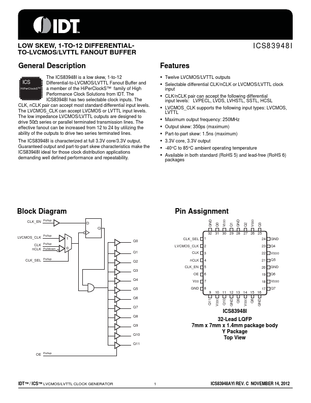
Block Diagram
CLK_EN Pullup
LVCMOS_CLK Pullup CLK Pullup n CLK Pulldown
CLK_SEL Pullup
1 0
OE Pullup
Q0
Q1 Q2 Q3 Q4 Q5 Q6 Q7 Q8 Q9 Q10 Q11
Pin Assignment
GND Q0 VDDO Q1 GND Q2 VDDO Q3
CLK_SEL LVCMOS_CLK
CLK n CLK CLK_EN
OE VDD...