ICS87421I
ICS87421I is DIFFERENTIAL-TO-LVDS CLOCK GENERATOR manufactured by Integrated Device Technology.
..
÷1/÷2 DIFFERENTIAL-TO-LVDS CLOCK GENERATOR
GENERAL DESCRIPTION
The ICS87421I is a high perfor mance ÷1/÷2 IC S Differential-to-LVDS Clock Generator and a mem Hi Per Clock S™ ber of the Hi Per Clock S™ family of High Performance Clock Solutions from IDT. The CLK, n CLK pair can accept most standard differential input levels. The ICS87421I is characterized to operate from a 3.3V power supply. Guaranteed part-to-part skew characteristics make the ICS87421I ideal for those clock distribution applications demanding well defined performance and repeatability.
Features
- One differential LVDS output
- One differential CLK, n CLK input pair
- CLK, n CLK pair can accept the following differential input levels: LVPECL, LVDS, LVHSTL, SSTL, HCSL
- Maximum clock input frequency: 1GHz
- Translates any single ended input signal (LVCMOS, LVTTL, GTL) to LVDS levels with resistor bias on n CLK input
- Part-to-part skew: 500ps (maximum)
- Propagation delay: 1.7ns (maximum)
- Additive phase jitter, RMS @ 155.52MHz: 0.17ps (typical)
- Full 3.3V operating supply
- -40°C to 85°C ambient operating temperature
- Available in both standard (Ro HS 5) and lead-free (Ro HS 6) packages
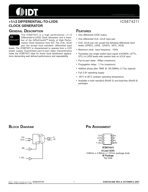
BLOCK DIAGRAM
CLK n CLK
PIN ASSIGNMENT
÷1 0 1
Q n Q CLK n CLK MR F_SEL 1 2 3 4 8 7 6 5 VDD Q n Q GND
R ÷2
8-Lead SOIC 3.90mm x 4.90mm x 1.37mm package body M Package Top View
F_SEL
IDT ™ / ICS™ LVDS CLOCK GENERATOR
ICS87421AMI REV. A OCTOBER 3, 2007
ICS87421I ÷1/÷2 DIFFERENTIAL-TO-LVDS CLOCK GENERATOR
..
TABLE 1. PIN DESCRIPTIONS
Number 1 2 3 Name CLK n CLK MR Input Input Input Type Pullup Description Pulldown Non-inver ting differential clock input. Inver ting differential clock input. Active High Master Reset. When logic HIGH, the internal dividers are reset causing the true output (Q) to go low and the inver ted output Pulldown (n Q) to go high. When logic LOW, the internal dividers and the output are enabled. LVCMOS / LVTTL interface levels. See Table...