Datasheet4U Logo Datasheet4U.com

IDT5T93GL10 - 2.5V LVDS 1:10 GLITCHLESS CLOCK BUFFER TERABUFFER II

General Description

APPLICATIONS:

The IDT5T93GL10 2.5V differential clock buffer is a user-selectable differential input to ten LVDS outputs .

Key Features

  • IDT5T93GL10 Guaranteed Low Skew < 25ps (max) Very low duty cycle distortion < 100ps (max) High speed propagation delay < 2ns (max) Up to 650MHz operation Glitchless input clock switching Selectable inputs Hot insertable and over-voltage tolerant inputs 3.3V / 2.5V LVTTL, HSTL, eHSTL,.

📥 Download Datasheet

Datasheet Details

Part number IDT5T93GL10
Manufacturer Integrated Device Technology
File Size 216.41 KB
Description 2.5V LVDS 1:10 GLITCHLESS CLOCK BUFFER TERABUFFER II
Datasheet download datasheet IDT5T93GL10 Datasheet

Full PDF Text Transcription (Reference)

The following content is an automatically extracted verbatim text from the original manufacturer datasheet and is provided for reference purposes only.

View original datasheet text
IDT5T93GL10 2.5V LVDS 1:10 GLITCHLESS CLOCK BUFFER TERABUFFER II INDUSTRIAL TEMPERATURE RANGE www.DataSheet4U.com 2.5V LVDS 1:10 GLITCHLESS CLOCK BUFFER TERABUFFER™ II
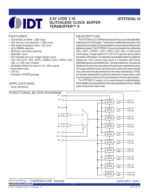
 FEATURES: • • • • • • • • • • • • IDT5T93GL10 Guaranteed Low Skew < 25ps (max) Very low duty cycle distortion < 100ps (max) High speed propagation delay < 2ns (max) Up to 650MHz operation Glitchless input clock switching Selectable inputs Hot insertable and over-voltage tolerant inputs 3.3V / 2.5V LVTTL, HSTL, eHSTL, LVEPECL (2.5V), LVPECL (3.3V), CML, or LVDS input interface Selectable differential inputs to ten LVDS outputs Power-down mode 2.5V VDD Available in VFQFPN package DESCRIPTION: APPLICATIONS: • Clock distribution The IDT5T93GL10 2.