IDT72V12071
IDT72V12071 is (IDT72V1x071) 3.3 VOLT DUAL MULTIMEDIA FIFO manufactured by Integrated Device Technology.
- Part of the IDT72V10071 comparator family.
- Part of the IDT72V10071 comparator family.
..
3.3 VOLT DUAL MULTIMEDIA FIFO DUAL 256 x 8, DUAL 512 x 8 DUAL 1,024 x 8, DUAL 2,048 x 8 DUAL 4,096 x 8
IDT72V10071, IDT72V11071 IDT72V12071, IDT72V13071 IDT72V14071
Features
- -
- -
- -
- -
- Memory organization: IDT72V10071 Dual 256 x 8 IDT72V11071 Dual 512 x 8 IDT72V12071 Dual 1,024 x 8 IDT72V13071 Dual 2,048 x 8 IDT72V14071 Dual 4,096 x 8 Offers optimal bination of large capacity, high speed, design flexibility and small footprint 15 ns read/write cycle time 5V input tolerant Separate control lines and data lines for each FIFO Separate Empty and Full flags for each FIFO Enable puts output data lines in high-impedance state Space-saving 64-pin plastic Thin Quad Flat Pack (STQFP) Industrial temperature range (- 40°C to +85° C)
DESCRIPTION
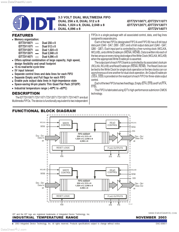
The IDT72V10071/72V11071/72V12071/72V13071/72V14071 are dual Multimedia FIFOs. The device is functionally equivalent to two independent
FIFOs in a single package with all associated control, data, and flag lines assigned to separate pins. Each of the two FIFOs (designated FIFO A and FIFO B) has a 8-bit input data port (DA0
- DA7, DB0
- DB7) and a 8-bit output data port (QA0
- QA7, QB0
- QB7). Each input port is controlled by a free-running clock (WCLKA, WCLKB), and a Write Enable pin (WENA, WENB). Data is written into each of the two arrays on every rising clock edge of the Write Clock (WCLKA, WCLKB) when the appropriate Write Enable pin is asserted. The output port of each FIFO bank is controlled by its associated clock pin (RCLKA, RCLKB) and Read Enable pin (RENA, RENB). The Read Clock can be tied to the Write Clock for single clock operation or the two clocks can run asynchronous of one another for dual clock operation. An Output Enable pin (OEA, OEB) is provided on the read port of each FIFO for three-state output control. Each of the two FIFOs has two fixed flags, Empty (EFA, EFB) and Full (FFA, FFB). This FIFO is fabricated using IDT's high-performance submicron CMOS technology.
FUNCTI...