IDTCV104B - CLOCK GENERATOR FOR DESKTOP PC PLATFORMS
Integrated Device Technology
General Description
KEY SPECIFICATION:
CPU/SRC CLK cycle to cycle jitter < 125ps SATA CLK cycle to cycle jitter < 125ps PCI CLK cycle to cycle jitter < 250ps Static PLL frequency divide error as low as 36ppm
FUNCTIONAL BLOCK DIAGRAM
DataSheet4U.com
PLL1 SSC EasyN Programming
Key Features
4 PLL architecture Linear frequency programming Independent frequency programming and SSC control Band-gap circuit for differential output High power-noise rejection ratio 66MHz to 533MHz CPU frequency VCO frequency up to 1.1G Support index block read/write, single cycle index block read Programmable REF, 3V66, PCI, 48MHz I/O drive strength Programmable 3V66 and PCI Skew Available in S.
Full PDF Text Transcription for IDTCV104B (Reference)
Note: Below is a high-fidelity text extraction (approx. 800 characters) for
IDTCV104B. For precise diagrams, and layout, please refer to the original PDF.
www.DataSheet4U.com IDTCV104B CLOCK GENERATOR FOR DESKTOP PC PLATFORMS COMMERCIAL TEMPERATURE RANGE CLOCK GENERATOR FOR DESKTOP PC PLATFORMS IDTCV104B PRELIMINARY FEATURE...
View more extracted text
CLOCK GENERATOR FOR DESKTOP PC PLATFORMS IDTCV104B PRELIMINARY FEATURES: • • • • • • • • • • • 4 PLL architecture Linear frequency programming Independent frequency programming and SSC control Band-gap circuit for differential output High power-noise rejection ratio 66MHz to 533MHz CPU frequency VCO frequency up to 1.1G Support index block read/write, single cycle index block read Programmable REF, 3V66, PCI, 48MHz I/O drive strength Programmable 3V66 and PCI Skew Available in SSOP package IDTCV104B is a 48 pin clock generation device for desktop PC platforms. 
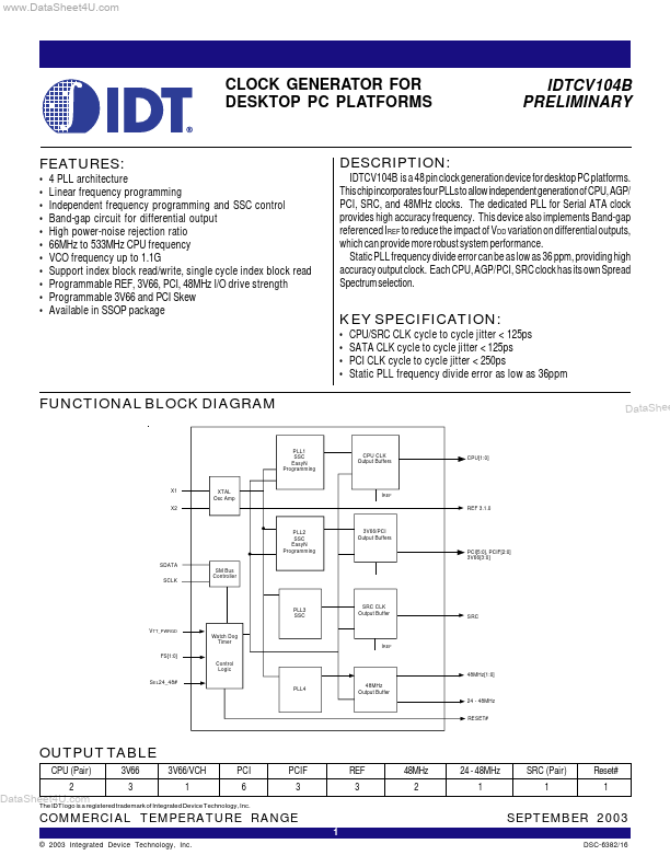
This chip incorporates four PLLs to allow independent generatio