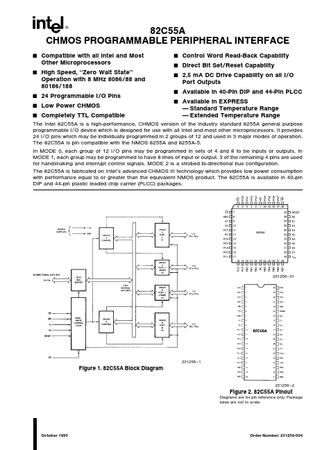
82C55A
Description
Symbol PA3- 0 RD CS Pin Number Dip PLCC 1- 4 5 6 2- 5 6 7 Type I O I I Name and Function PORT A PINS 0
- 3 Lower nibble of an 8-bit data output latch buffer and an 8-bit data input latch READ CONTROL This input is low during CPU read operations CHIP SELECT A low on this input enables the 82C55A to respond to RD and WR signals RD and WR are ignored otherwise System Ground I ADDRESS These input signals in conjunction RD and WR control the selection of one of the three ports or the control word registers A1 0 0 1 1 0 0 1 1 X X PC7- 4 10- 13 11 13- 15 I O A0 0 1 0 1 0 1 0 1 X X RD 0 0 0 0 1 1 1 1 X 1 WR 1 1 1 1 0 0 0 0 X 1 CS 0 0 0 0 0 0 0 0 1 0 Input Operation (Read) Port A
- Data Bus Port B
- Data Bus Port C
- Data Bus Control Word
- Data Bus Output Operation (Write) Data Bus
- Port A Data Bus
- Port B Data Bus
- Port C Data Bus
- Control Disable Function Data Bus
- 3
- State Data Bus
- 3
- State
GND A1- 0
7 8- 9
8 9- 10
PORT C PINS 4
- 7 Upper nibble of an 8-bit data output...