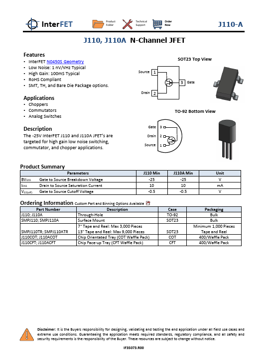
| Part | J110A |
|---|---|
| Description | N-Channel JFET |
| Manufacturer | InterFET Corporation |
| Size | 817.86 KB |
Related Datasheets
| Part Number | Manufacturer | Description |
|---|---|---|
| J110A | Siliconix | n-channel JFET |
| J110 | Fairchild Semiconductor | N-Channel Switch |
| J110 | onsemi | JFET - General Purpose N-Channel |
| J110 | Motorola Semiconductor | JFET GENERAL-PURPOSE TRANSISTOR |
| J110 | Vishay | N-Channel JFETs |


