InterFET IFN113
IFN113 is a low noise high gain replacement for the Japanese 2SK113 JFET. The TO-18 package is hermetically sealed and suitable for military applications.| Part No. | IFN113 |
|---|---|
| Datasheet | IFN113 Download |
| Manufacturer |  InterFET |
| Description | N-Channel JFET |
| Buy | Stock & Price |

FEATURES
● InterFET N0132S Geometry● Low Noise: 1.2 nV/√Hz Typical
● High Gain: 15mS Typical
● RoHS Compliant
● SMT, TH, and Bare Die Package options.
APPLICATIONS
● Low-Noise, High Gain● Replacement for Japanese 2SK113
DESCRIPTION
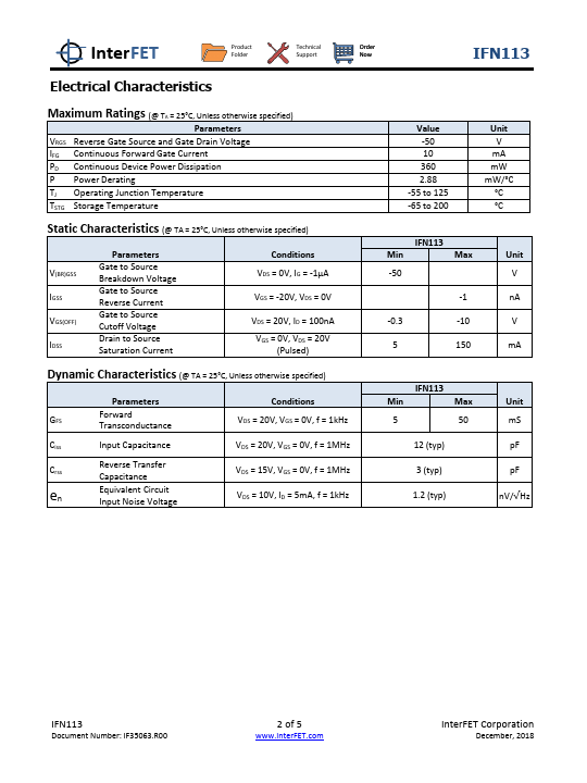
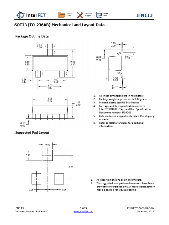
The -50V InterFET Gate leakages are typically less than 50pA at room temperatures. Gate/Case Drain 2 Source TO-18 Bottom View 3 1 Source 1 Drain 2 SOT23 Top View 3 Gate TO-92 Bottom View Gate 3 Drain 2 Source 1 Product Summary Parameters BVGSS Gate to Source Breakdown Voltage IDSS Drain to Source Saturation Current VGS(off) Gate to Source Cutoff Voltage GFS Forward Transconductance Ordering Information Custom Part and Binning Options Available Part NumberDESCRIPTION
IFN113 Through-Hole PN113 Through-Hole SMP113 Surface Mount 7“ Tape and Reel: Max 3,000 Pieces SMP113TR 13” Tape and Reel: Max 9,000 Pieces IFN113COT Chip Orientated Tray (COT Waffle Pack) IFN113CFT Chip Face-up Tray (CFT Waffle Pack) IFN113 Min Unit -50 V 5 mA -0.3 V 5 mS Case TO-18 TO-92 SOT...