IP2003A
IP2003A is Synchronous Buck Multiphase Optimized LGA Power Block Integrated Power Semiconductors manufactured by International Rectifier.
Features
:
Integrated Power Semiconductors, Drivers & Passives
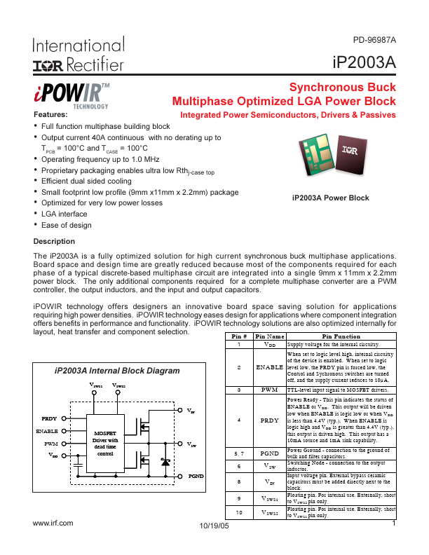
Full function multiphase building block Output current 40A continuous with no derating up to TPCB = 100°C and TCASE = 100°C Operating frequency up to 1.0 MHz Proprietary packaging enables ultra low Rthj-case top Efficient dual sided cooling Small footprint low profile (9mm x11mm x 2.2mm) package Optimized for very low power losses LGA interface Ease of design i P2003A Power Block
Description
The i P2003A is a fully optimized solution for high current synchronous buck multiphase applications. Board space and design time are greatly reduced because most of the ponents required for each phase of a typical discrete-based multiphase circuit are integrated into a single 9mm x 11mm x 2.2mm power block. The only additional ponents required for a plete multiphase converter are a PWM controller, the output inductors, and the input and output capacitors. i POWIR technology offers designers an innovative board space saving solution for applications requiring high power densities. i POWIR technology eases design for applications where ponent integration offers benefits in performance and functionality. i POWIR technology solutions are also optimized internally for layout, heat transfer and ponent selection.
Pin #
Pin N am e Pin Function V DD Supply voltage for the internal circuitry. i P2003A Internal Block Diagram
VSWS1 VSWS2
ENA BLE
W hen set to logic level high, internal circuitry of the device is enabled. W hen set to logic level low, the PRD Y pin is forced low, the Control and Sychronous switches are turned off, and the supply current reduces to 10µ A. T T L-level input signal to M OSFET drivers. Power Ready
- This pin indicates the status of EN AB LE or V D D . T his output will be driven low when EN ABLE is logic low or when V D D is less than 4.4V (typ.). W hen EN AB LE is logic high and V D D is greater than 4.4V (typ.), this output is driven high. T his output has a 10m A source...