IRF8910PBF
IRF8910PBF is HEXFET Power MOSFET manufactured by International Rectifier.
PD -95673
HEXFET® Power MOSFET
Applications l Dual SO-8 MOSFET for POL converters in desktop, servers, graphics cards, game consoles and set-top box l
VDSS
20V
13.4m:@VGS = 10V
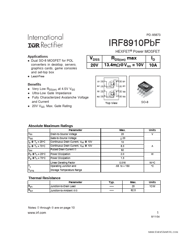
1 2 3 4
RDS(on) max
10A
Lead-Free
S1 G1 S2 G2
8 7 6 5
Benefits l Very Low RDS(on) at 4.5V VGS l Ultra-Low Gate Impedance l Fully Characterized Avalanche Voltage and Current l 20V VGS Max. Gate Rating
D1 D1 D2 D2
Top...