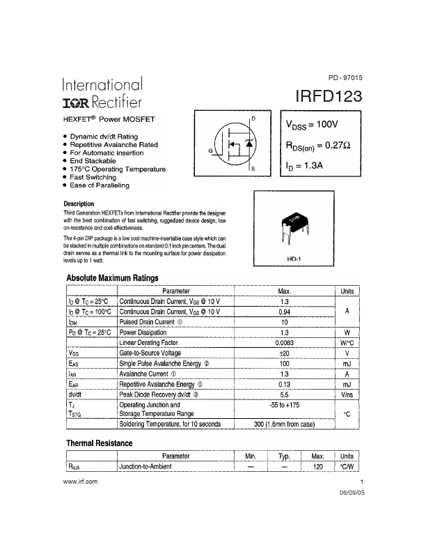
IRFD123
IRFD123 is N-Channel Power MOSFET manufactured by International Rectifier.
- 97015
.irf.
1 06/09/05
.irf.
.irf.
.irf.
.irf.
.irf.
Peak Diode Recovery dv/dt Test Circuit
+
Circuit Layout Considerations
- Low Stray Inductance
- Ground Plane
- Low Leakage Inductance Current Transformer
+ +
- - dv/dt controlled by RG
- ISD controlled by Duty Factor "D"
- D.U.T.
- Device Under Test
+
- -
Reverse Polarity for P-Channel
- - Use P-Channel Driver for P-Channel Measurements
Driver Gate Drive P.W. Period D=
P.W. Period VGS=10V
D.U.T. ISD Waveform Reverse Recovery Current Body Diode Forward Current di/dt D.U.T. VDS Waveform Diode Recovery dv/dt
Re-Applied Voltage Inductor Curent
Body Diode
Forward Drop
Ripple ≤ 5%
- -
- VGS = 5.0V for Logic Level and 3V Drive Devices Fig -14 For N Channel HEXFETS
.irf.
Hexdip Package Outline
Dimensions are shown in millimeters (inches)
Hexdip Part Marking Information
UCDTÃDTÃ6IÃDSA9 ! DIU@SI6UDPI6G S@8UDAD@S GPBP...