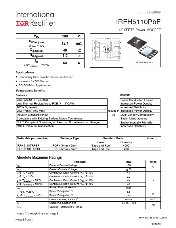
IRFH5110PBF
IRFH5110PBF is HEXFET Power MOSFET manufactured by International Rectifier.
Features and Benefits
Features
Benefits
Low RDSon (< 12.4 mΩ) Low Thermal Resistance to PCB (< 1.1°C/W) 100% Rg tested Low Profile (<0.9 mm) Industry-Standard Pinout patible with Existing Surface Mount Techniques Ro HS pliant Containing no Lead, no Bromide and no Halogen MSL1, Industrial Qualification
Lower Conduction Losses Increased Power Density Increased Reliability results in Increased Power Density ⇒ Multi-Vendor patibility Easier Manufacturing Environmentally Friendlier Increased Reliability
Orderable part number IRFH5110TRPBF IRFH5110TR2PBF
Package Type PQFN 5mm x 6mm PQFN 5mm x 6mm
Standard Pack Form Quantity Tape and Reel 4000 Tape and Reel 400
Note
Absolute Maximum Ratings
VDS VGS ID @ TA = 25°C ID @ TA = 70°C ID @ TC(Bottom) = 25°C ID @ TC(Bottom) = 100°C IDM PD @TA = 25°C PD @ TC(Bottom) = 25°C TJ TSTG Parameter Drain-to-Source Voltage Gate-to-Source Voltage Continuous Drain Current, VGS @ 10V Continuous Drain Current, VGS @ 10V Continuous Drain Current, VGS @ 10V Continuous Drain Current, VGS @ 10V Pulsed Drain Current Power Dissipation Power Dissipation Max. 100 ± 20 11 9.0 63 40 252 3.6 114 0.029 -55 to + 150 Units V
A g g c
W W/°C °C
Linear Derating Factor Operating Junction and Storage Temperature Range g
Notes through
are on page 8
.irf.
03/18/10
IRFH5110Pb F
BVDSS ∆ΒVDSS/∆TJ RDS(on) VGS(th) ∆VGS(th) IDSS IGSS gfs Qg Qgs1 Qgs2 Qgd Qgodr Qsw Qoss RG td(on) tr td(off) tf Ciss Coss Crss
..
Static @ TJ = 25°C (unless otherwise specified)
Parameter Drain-to-Source Breakdown Voltage Breakdown Voltage Temp. Coefficient Static Drain-to-Source On-Resistance Gate Threshold Voltage Gate Threshold Voltage Coefficient Drain-to-Source Leakage Current Gate-to-Source Forward Leakage Gate-to-Source Reverse Leakage Forward Transconductance Total Gate Charge Pre-Vth Gate-to-Source Charge Post-Vth Gate-to-Source Charge Gate-to-Drain Charge Gate Charge Overdrive Switch Charge (Qgs2 + Qgd) Output Charge Gate Resistance Turn-On Delay Time Rise...