CD4001BMS
Description
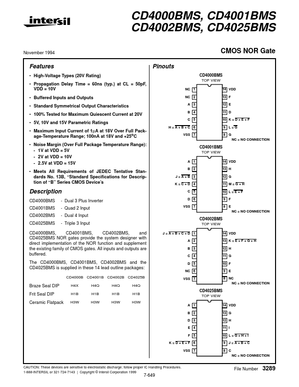
CD4000BMS CD4001BMS CD4002BMS CD4025BMS - Dual 3 Plus Inverter - Quad 2 Input - Dual 4 Input - Triple 3 Input CD4002BMS TOP VIEW J=A+B+C+D 1 A 2 B 3 C 4 D 5 NC 6 VSS 7 14 VDD 13 K = E + F + G + H 12 H 11 G 10 F 9 E 8 NC NC = NO CONNECTION CD4000BMS, CD4001BMS, CD4002BMS, and CD4025BMS NOR gates provide the system designer with direct implementation of the NOR function and supplement the existing family of CMOS gates.
Key Features
- High-Voltage Types (20V Rating)
- Propagation Delay Time = 60ns (typ.) at CL = 50pF, VDD = 10V
- Buffered Inputs and Outputs
- Standard Symmetrical Output Characteristics
- 100% Tested for Maximum Quiescent Current at 20V
- Maximum Input Current of 1µA at 18V Over Full Package-Temperature Range; 100nA at 18V and +25oC
- Noise Margin (Over Full Package Temperature Range): - 1V at VDD = 5V - 2V at VDD = 10V - 2.5V at VDD = 15V