CD4019BMS
Description
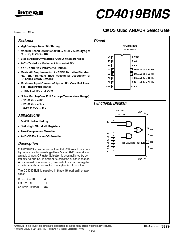
CD4019BMS types consist of four AND/OR select gate configurations, each consisting of two 2-input AND gates driving a single 2-input OR gate. Selection is accomplished by control bits Ka and Kb.
Key Features
- High Voltage Type (20V Rating)
- Medium Speed Operation tPHL = tPLH = 60ns (typ.) at CL = 50pF, VDD = 10V
- Standardized Symmetrical Output Characteristics
- 100% Tested for Quiescent Current at 20V
- 5V, 10V and 15V Parametric Ratings
- Meets All Requirements of JEDEC Tentative Standard No. 13B, “Standard Specifications for Description of ‘B’ Series CMOS Devices”
- Maximum Input Current of 1µa at 18V Over Full Package-Temperature Range; - 100nA at 18V and 25 oC
- Noise Margin (Over Full Package Temperature Range): - 1V at VDD = 5V - 2V at VDD = 10V - 2.5V at VDD = 15V