CD4082BMS Overview
Description
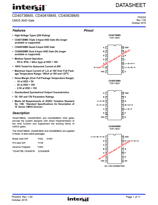
CD4073BMS, CD4081BMS and CD4082BMS AND gates provide the system designer with direct implementation of the AND function and supplement the existing family of CMOS gates. The CD4073BMS, CD4081BMS and CD4082BMS are supplied in these 14 lead outline packages: Braze Seal DIP Frit Seal DIP Ceramic Flatpack *CD4073B, CD4081B *H4Q *H1B *H3W †CD4082B †H4H C 5 D 6 VSS 7 CD4082BMS TOP VIEW J=A - B - C - D 1 D 2 C 3 B 4 A 5 NC 6 VSS 7 14 VDD 13 K = E - F - G - H 12 H 11 G 10 F 9 E 8 NC NC = NO CONNECTION CAUTION: These devices are sensitive to electrostatic discharge; follow proper IC Handling Procedures.
Key Features
- High-Voltage Types (20V Rating)
- CD4073BMS Triple 3-Input AND Gate
- CD4081BMS Quad 2-Input AND Gate
- CD4082BMS Dual 4-Input AND Gate
- Medium Speed Operation
- tPLH, tPHL = 60ns (typ) at VDD = 10V
- 100% Tested for Quiescent Current at 20V
- Maximum Input Current of 1µA at 18V Over Full Package Temperature Range; 100nA at 18V and +25oC
- Noise Margin (Over Full Package Temperature Range)
- 1V at VDD = 5V