CD4085BMS
Features
- High Voltage Type (20V Rating)
- Medium Speed Operation
- t PHL = 90ns
- t PLH = 125ns (Typ.) at 10V
- Individual Inhibit Controls
- 5V, 10V and 15V Parametric Ratings
- Standardized Symmetrical Output Characteristics
- 100% Tested for Quiescent Current at 20V
- Maximum Input Current of 1µA at 18V Over Full Package Temperature Range; 100n A at 18V and +25o C
- Noise Margin (Over Full Package/Temperature Range)
- 1V at VDD = 5V
- 2V at VDD = 10V
- 2.5V at VDD = 15V
- Meets All Requirements of JEDEC Tentative Standard No. 13B, “Standard Specifications for Description of ‘B’ Series CMOS Devices”
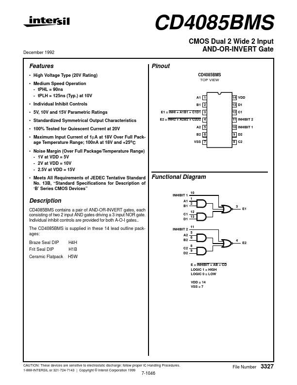
A1 1 B1 2 E1 = INHI + A1B1 + C1D1 3 E2 = INH2 + A2B2 + C2D2 4 A2 5 B2 6 VSS 7
14 VDD 13 D1 12 C1 11 INHIBIT 2 10 INHIBIT 1 9 D2 8 C2
Functional Diagram
INHIBIT 1 10
Description
CD4085BMS contains a pair of AND-OR-INVERT gates, each consisting of two 2 input AND gates driving a 3 input NOR gate. Individual inhibit controls are provided for both A-O-I gates.. The CD4085BMS is supplied in...