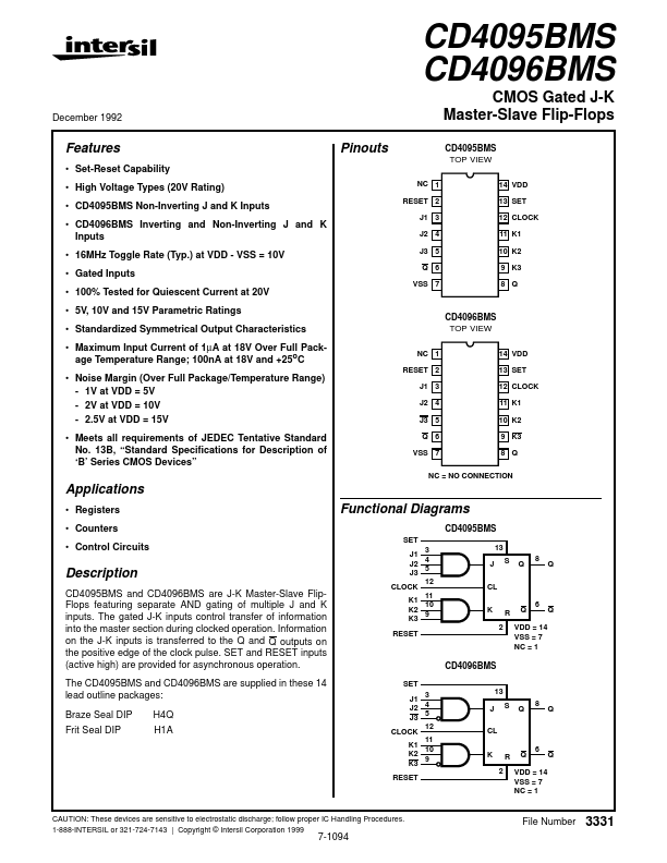
Datasheet4U Logo Datasheet4U.com

CD4095BMS - CMOS Gated J-K Master-Slave Flip-Flops

Datasheet Summary

Description

of ‘B’ Series CMOS Devices” CD4095BMS TOP VIEW 14 VDD 13 SET 12 CLOCK 11 K1 10 K2 9 K3 8 Q CD4096BMS TOP VIEW NC 1 RESET 2 J1 3 J2 4 J3 5 Q 6 VSS 7 14 VDD 13 SET 12 CLOCK 11 K1 10 K2 9 K3 8 Q NC = NO CONNECTION Applications Registers Counters Control Circuits SET 3

Features

  • Set-Reset Capability.
  • High Voltage Types (20V Rating).
  • CD4095BMS Non-Inverting J and K Inputs.
  • CD4096BMS Inverting and Non-Inverting J and K Inputs.
  • 16MHz Toggle Rate (Typ. ) at VDD - VSS = 10V.
  • Gated Inputs.
  • 100% Tested for Quiescent Current at 20V.
  • 5V, 10V and 15V Parametric Ratings.
  • Standardized Symmetrical Output Characteristics.
  • Maximum Input Current of 1µA at 18V Over Full Package Temperature Range; 1.

📥 Download Datasheet

Datasheet preview – CD4095BMS

Datasheet Details

Part number CD4095BMS
Manufacturer Intersil Corporation
File Size 101.13 KB
Description CMOS Gated J-K Master-Slave Flip-Flops
Datasheet download datasheet CD4095BMS Datasheet
Additional preview pages of the CD4095BMS datasheet.
Other Datasheets by Intersil Corporation

Full PDF Text Transcription

Click to expand full text
CD4095BMS CD4096BMS December 1992 CMOS Gated J-K Master-Slave Flip-Flops Pinouts NC 1 RESET 2 J1 3 J2 4 J3 5 Q 6 VSS 7 Features • Set-Reset Capability • High Voltage Types (20V Rating) • CD4095BMS Non-Inverting J and K Inputs • CD4096BMS Inverting and Non-Inverting J and K Inputs • 16MHz Toggle Rate (Typ.) at VDD - VSS = 10V • Gated Inputs • 100% Tested for Quiescent Current at 20V • 5V, 10V and 15V Parametric Ratings • Standardized Symmetrical Output Characteristics • Maximum Input Current of 1µA at 18V Over Full Package Temperature Range; 100nA at 18V and +25oC • Noise Margin (Over Full Package/Temperature Range) - 1V at VDD = 5V - 2V at VDD = 10V - 2.5V at VDD = 15V • Meets all requirements of JEDEC Tentative Standard No.
Published: |