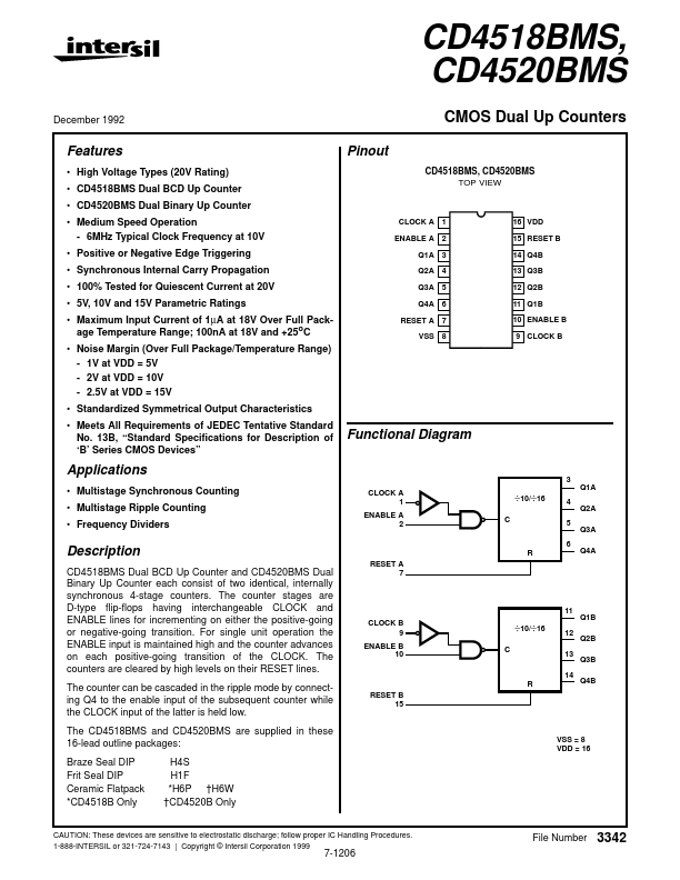
Datasheet4U Logo Datasheet4U.com

CD4518BMS - CMOS Dual Up Counters

General Description

of ‘B’ Series CMOS Devices” CLOCK A ENABLE A Q1A Q2A Q3A Q4A RESET A VSS 1 2 3 4 5 6 7 8 16 VDD 15 RESET B 14 Q4B 13 Q3B 12 Q2B 11 Q1B 10 ENABLE B 9 CLOCK B Functional Diagram Applications 3 Multistage Synchronous Counting Multistage Ripple Counting Frequency Divi

Key Features

  • High Voltage Types (20V Rating).
  • CD4518BMS Dual BCD Up Counter.
  • CD4520BMS Dual Binary Up Counter.
  • Medium Speed Operation - 6MHz Typical Clock Frequency at 10V.
  • Positive or Negative Edge Triggering.
  • Synchronous Internal Carry Propagation.
  • 100% Tested for Quiescent Current at 20V.
  • 5V, 10V and 15V Parametric Ratings.
  • Maximum Input Current of 1µA at 18V Over Full Package Temperature Range; 100nA at 18V and +25oC.

📥 Download Datasheet

Full PDF Text Transcription (Reference)

The following content is an automatically extracted verbatim text from the original manufacturer datasheet and is provided for reference purposes only.

View original datasheet text
CD4518BMS, CD4520BMS December 1992 CMOS Dual Up Counters Pinout CD4518BMS, CD4520BMS TOP VIEW Features • High Voltage Types (20V Rating) • CD4518BMS Dual BCD Up Counter • CD4520BMS Dual Binary Up Counter • Medium Speed Operation - 6MHz Typical Clock Frequency at 10V • Positive or Negative Edge Triggering • Synchronous Internal Carry Propagation • 100% Tested for Quiescent Current at 20V • 5V, 10V and 15V Parametric Ratings • Maximum Input Current of 1µA at 18V Over Full Package Temperature Range; 100nA at 18V and +25oC • Noise Margin (Over Full Package/Temperature Range) - 1V at VDD = 5V - 2V at VDD = 10V - 2.5V at VDD = 15V • Standardized Symmetrical Output Characteristics • Meets All Requirements of JEDEC Tentative Standard No.