Datasheet Summary
December 1992
CMOS Quad Clocked “D” Latch
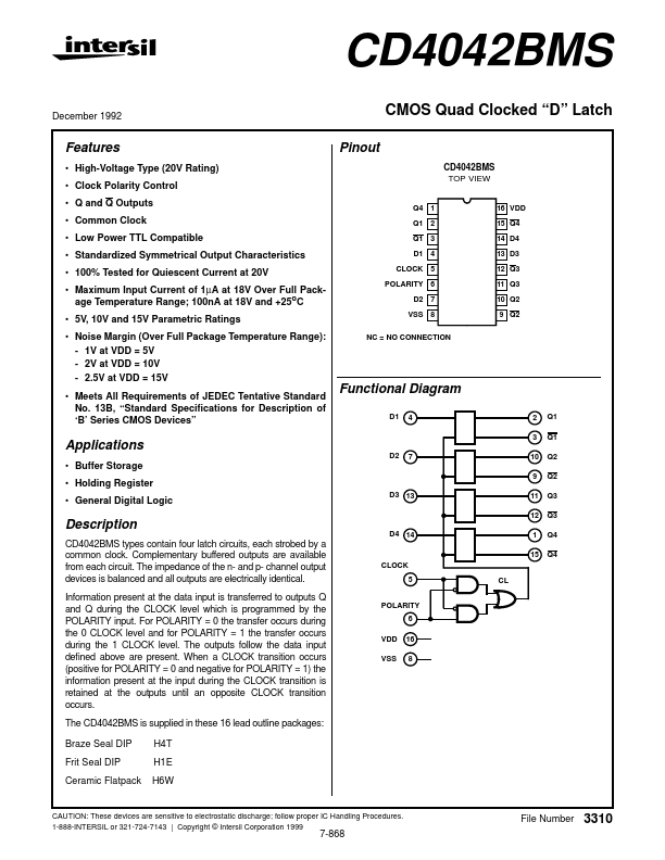
Pinout
CD4042BMS TOP VIEW
Features
- High-Voltage Type (20V Rating)
- Clock Polarity Control
- Q and Q Outputs
- mon Clock
- Low Power TTL patible
- Standardized Symmetrical Output Characteristics
- 100% Tested for Quiescent Current at 20V
- Maximum Input Current of 1µA at 18V Over Full Package Temperature Range; 100nA at 18V and +25oC
- 5V, 10V and 15V Parametric Ratings
- Noise Margin (Over Full Package Temperature Range):
- 1V at VDD = 5V
- 2V at VDD = 10V
- 2.5V at VDD = 15V
- Meets All Requirements of JEDEC Tentative Standard No. 13B, “Standard Specifications for Description of ‘B’ Series CMOS Devices”
Q4 1 Q1 2 Q1 3 D1 4...