MAXIMUM RATINGS
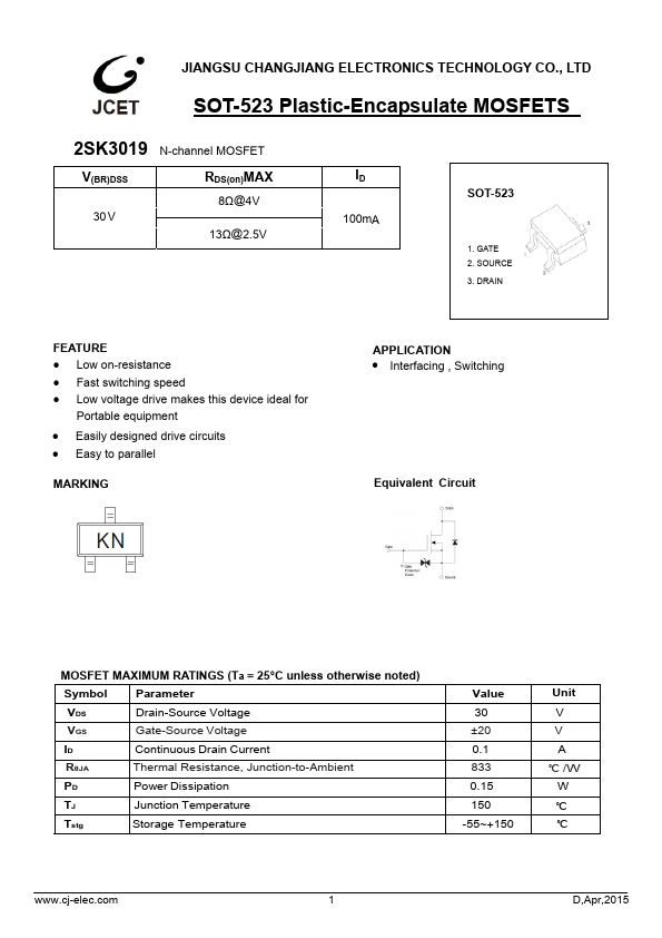
(Ta = 25°C unless otherwise noted) Symbol Parameter VDS Drain-Source Voltage VGS Gate-Source Voltage ID Continuous Drain Current RθJA Thermal Resistance, Junction-to-Ambient PD Power Dissipation TJ Junction Temperature Tstg Storage Temperature Value 30 ±20 0.1 833 0.15 150 -55~+150 Unit V V A ℃ /W W ℃ ℃ 1 D,Apr,2015 MOSFET ELECTRICAL CHARACTERISTICS
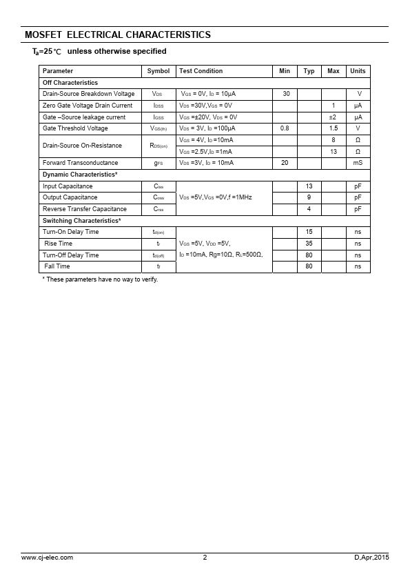
Ta=25 ℃ unless otherwise specified Parameter Off Characteristics Drain-Source Breakdown Voltage Zero Gate Voltage Drain Current Gate –Source leakage current Gate Threshold Voltage Symbol VDS IDSS IGSS VGS(th) Drain-Source On-Resistance RDS(on) Forward Transconductance gFS Dynamic Characteristics* Input Capacitance Ciss Output Capacitance Coss Reverse Transfer Capacitance Crss Switching Characteristics* Turn-On Delay Time td(on) Rise Time Turn-Off Delay Time tr td(off) Fall Time tf * These parameters have no way to verify. Test Condition VGS = 0V, ID = 10µA VDS =30V,VGS = 0V VGS =±20V, VDS = 0V VDS = 3V, ID =100µA VGS = 4V, ID =10mA VGS =2.5V,ID =1mA VDS =3V, ID = 10mA VDS =5V,VGS =0V,f =1MHz VGS =5V, VDD =5V, ID =10mA, Rg=10Ω, RL=500Ω, Min Typ Max Units 30 V 1 µA ±2 µA 0. JCET