JCET CJ1012
This Single N-Channel MOSFET has been designed using advanced 3.| Part No. | CJ1012 |
|---|---|
| Datasheet | CJ1012 Download |
| Manufacturer |  JCET |
| Description | N-Channel MOSFET |
| Buy | Stock & Price |
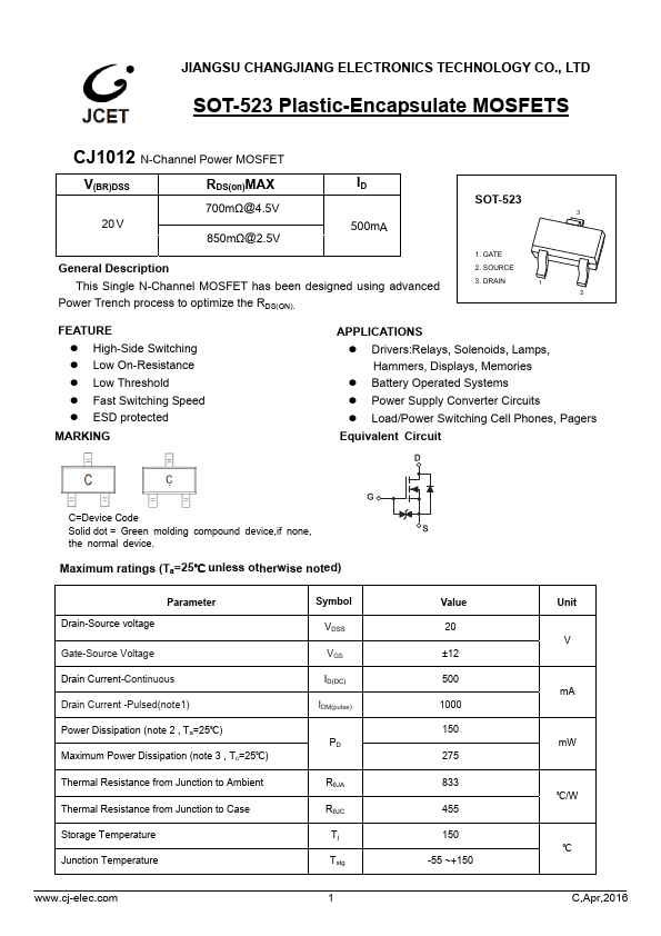
GENERAL DESCRIPTION
2. SOURCE DRAIN 1 2 Power Trench process to optimize the RDS(ON). FEATURE● High-Side Switching
● Low On-Resistance
● Low Threshold
● Fast Switching Speed
● ESD protected MARKING
APPLICATIONS
● Drivers:Relays, Solenoids, Lamps, Hammers, Displays, Memories● Battery Operated Systems
● Power Supply Converter Circuits
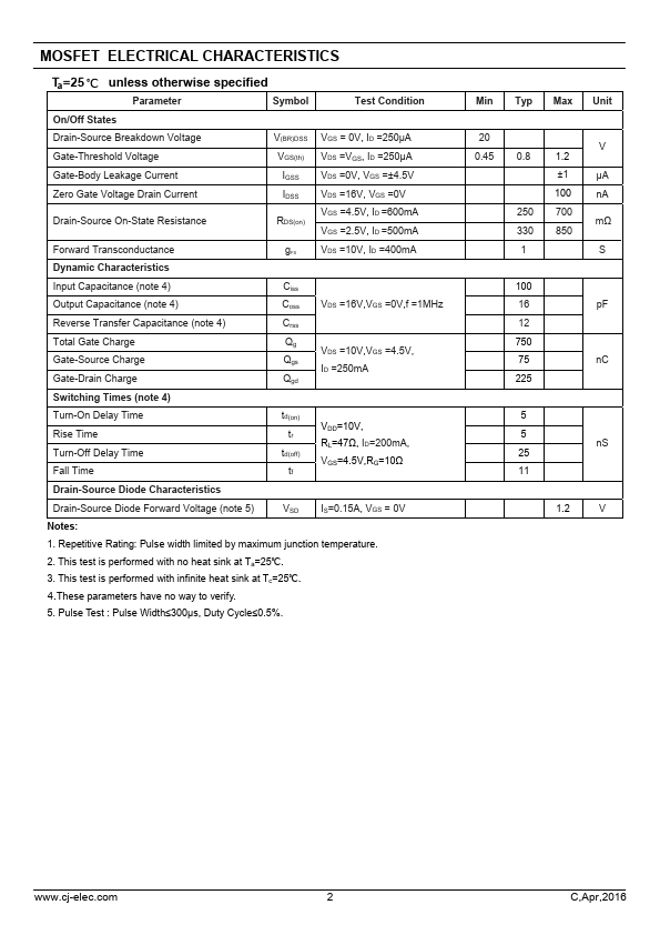
● Load/Power Switching Cell Phones, Pagers Equivalent Circuit C= Device Code Solid dot = Green molding compound device,if none, the normal device. Maximum ratings (Ta=25℃ unless otherwise noted) Parameter Drain-Source voltage Gate-Source Voltage Drain Current-Continuous Drain Current -Pulsed(note1) Power Dissipation (note 2 , Ta=25℃) Maximum Power Dissipation (note 3 , Tc=25℃) Thermal Resistance from Junction to Ambient Thermal Resistance from Junction to Case Storage Temperature Junction Temperature Symbol VDSS VGS ID(DC) IDM(pulse) PD RθJA RθJC Tj Tstg 1 Value 20 ±12 500 1000 150 275 833 455 150 -55 ~+150 Unit V mA mW ℃/W ℃ C,Apr,2016 MOSFET ELECTRICAL...