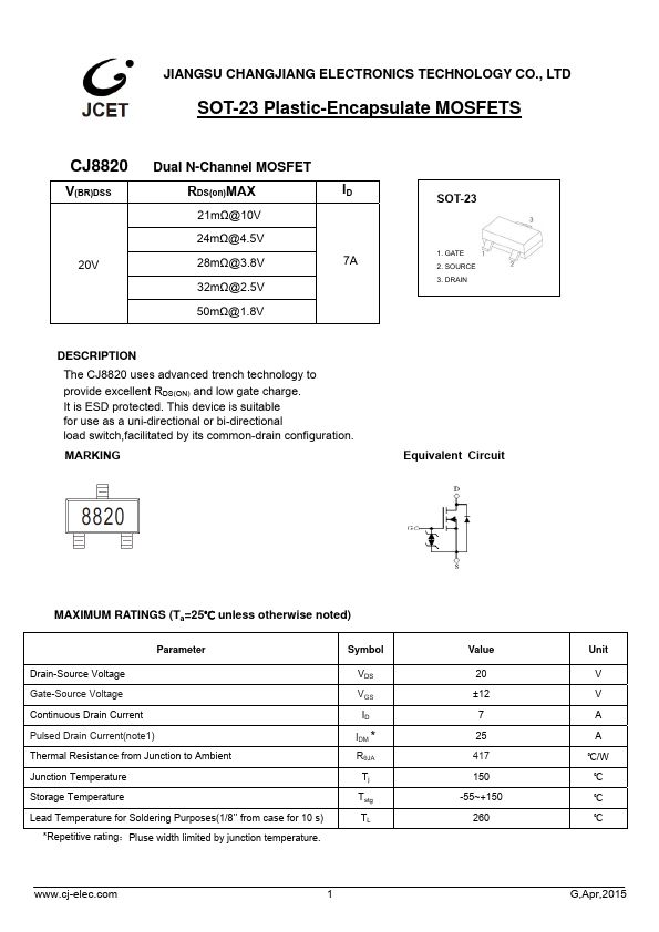
DESCRIPTION
It is ESD protected. MARKING SOT-23 1. GATE 2. SOURCE 3. DRAIN Equivalent Circuit MAXIMUM RATINGS
(Ta=25℃ unless otherwise noted) Parameter Drain-Source Voltage Gate-Source Voltage Continuous Drain Current Pulsed Drain Current(note1) Thermal Resistance from Junction to Ambient Junction Temperature Storage Temperature Lead Temperature for Soldering Purposes(1/8’’ from case for 10 s) *Repetitive rating:Pluse width limited by junction temperature. Symbol VDS VGS ID IDM * RθJA Tj Tstg TL 1 Value 20 ±12 7 25 417 150 -55~+150 260 Unit V V A A ℃/W ℃ ℃ ℃ G,Apr,2015 MOSFET ELECTRICAL CHARACTERISTICS
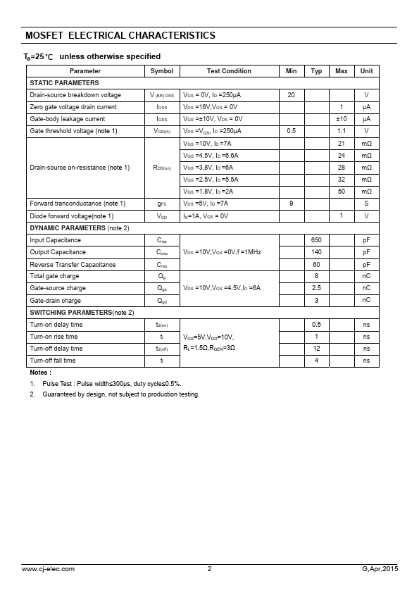
Ta=25 ℃ unless otherwise specified Parameter Symbol Test Condition STATIC PARAMETERS Drain-source breakdown voltage V (BR) DSS VGS = 0V, ID =250µA Zero gate voltage drain current IDSS VDS =16V,VGS = 0V Gate-body leakage current IGSS VGS =±10V, VDS = 0V Gate threshold voltage (note 1) VGS(th) VDS =VGS, ID =250µA VGS =10V, ID =7A VGS =4.5V, ID =6.6A Drain-source on-resistance (note 1) RDS(... JCET