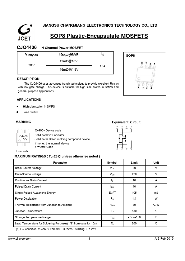
DESCRIPTION
APPLICATIONS
z High side switch in SMPS z Load Switch MARKING Q4406= Device code Solid dot=Pin1 indicator Solid dot = Green molding compound device, if none, the normal device YY=Date Code Front side MAXIMUM RATINGS
( Ta=25℃ unless otherwise noted ) Parameter Drain-Source Voltage Gate-Source Voltage Continuous Drain Current Pulsed Drain Current Single Pulsed Avalanche Energy Power Dissipation Thermal Resistance from Junction to Ambient Junction Temperature Storage Temperature Range Lead Temperature for Soldering Purposes(1/8’’ from case for 10s) (1).EAS condition: VDD=50V,L=0.5mH, RG=25Ω, Starting TJ = 25°C Equivalent Circuit D D D D 8 7 6 5 1 2 3 4 S S S G Symbol VDS VGS ID IDM EAS(1) PD RθJA TJ Tstg TL Limit 30 ±20 10 40 105 1.4 89 150 -55 ~+150 260 1 Unit V V A A mJ W ℃/W ℃ ℃ ℃ A-3,Feb,2016 MOSFET ELECTRICAL CHARACTERISTICS
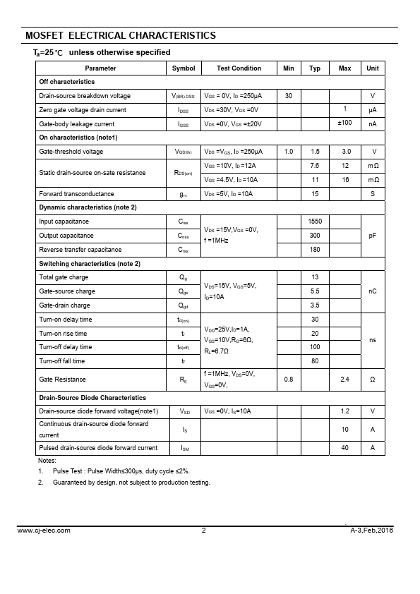
Ta=25 ℃ unless otherwise specified Parameter Symbol Test Condition Off characteristics Drain-source breakdown voltage Zero gate voltage drain current... JCET