JCET DAN217
SWITCHING DIODE
| Part No. | DAN217 |
|---|---|
| Datasheet | DAN217 Download |
| Manufacturer |  JCET |
| Description | SWITCHING DIODE |
| Buy | Stock & Price |

FEATURES
z Small surface mounting type z Two diode elements are connected in series MARKING: BA1 BA1 BA1 Solid dot = Green molding compound device,if none,the normal device.MAXIMUM RATINGS
@Ta=25℃ Parameter Non-Repetitive Peak Reverse Voltage DC Blocking Voltage Forward Continuous Current Non-Repetitive Peak Forward Surge Current @t=8.3ms Average Rectified Output Current Power Dissipation Thermal resistance From Junction to ambient Junction Temperature Storage Temperature Range Symbol VRM VR IFM IFSM IO PD RθJA TJ TSTG SOT-23 - 1 3 2 Limit 80 80 300 2.0 100 200 625 150 -55~+150 Unit V V mA A mA mW ℃/W ℃ ℃ELECTRICAL CHARACTERISTICS
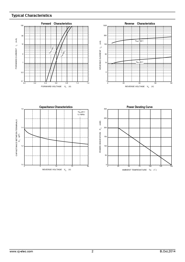
(Ta=25℃ unless otherwise specified) Parameter Reverse breakdown voltage Reversen voltage leakage current Forward voltage Symbol V(BR) IR VF Test conditions IR= 100μA VR=70V IF=100mA Min 80 Max 0.1 1.2 Unit V μA V 1 B,Oct,2014 FORWARD CURRENT I (mA) F Ta=100℃ Ta=25℃ REVERSE CURRENT I (nA) R Typical Characteristics Forward Characteristics 100 30 10 3 1 0.3 0.